Essential Considerations for PCB Design: What You Need to Know Before You Start
Printed Circuit Board (PCB) design is a critical step in electronic product development that bridges the conceptual and physical realization of electronic circuits. Whether you’re an electrical engineer, hobbyist, or student, understanding the key considerations before starting your PCB layout can save time, reduce costs, and improve the performance and reliability of your final product. This comprehensive guide explores the fundamental questions and decisions you’ll need to address when designing a PCB.
1. Understanding Your Design Requirements
Before opening your PCB design software, you must clearly define your project’s specifications and constraints.
1.1 Functional Requirements
- Circuit purpose: What is the primary function of your PCB? Is it for power regulation, signal processing, data acquisition, or another purpose?
- Performance specifications: What are the critical parameters (speed, power consumption, noise limits, etc.) that your design must meet?
- Operating environment: Will the PCB be used in extreme temperatures, high humidity, or other challenging conditions?
1.2 Physical Constraints
- Board dimensions: What are the maximum allowable length, width, and thickness of your PCB?
- Mounting requirements: How will the board be mounted in its enclosure? Are there specific fastener locations or standoff requirements?
- Connector placement: Where must external interfaces (power inputs, data connectors, etc.) be located for proper enclosure integration?
1.3 Regulatory Compliance
- Safety standards: Does your product need to meet specific safety certifications (UL, CE, etc.)?
- EMC/EMI requirements: Are there electromagnetic compatibility standards your design must satisfy?
- Environmental regulations: Does your product need to comply with RoHS, WEEE, or other environmental directives?
2. Schematic Design Considerations
The schematic is the foundation of your PCB design and requires careful attention before proceeding to layout.
2.1 Component Selection
- Availability and lead time: Are your chosen components readily available, or do they have long procurement times?
- Package types: Have you considered the PCB footprint requirements of each component (SMD vs. through-hole, pitch sizes, etc.)?
- Alternative parts: Have you identified acceptable alternates for components that might be unavailable?
2.2 Circuit Partitioning
- Functional blocks: Can your design be logically divided into sections (power supply, digital processing, analog I/O, etc.)?
- Signal flow: Is your schematic organized to show clear signal paths from inputs to outputs?
- Hierarchical design: For complex circuits, would a hierarchical schematic structure improve readability and maintainability?
2.3 Design Verification
- Electrical rules: Have you verified voltage levels, current requirements, and power dissipation for all components?
- Simulation: Would circuit simulation help validate performance before committing to PCB layout?
- Design review: Have you had another engineer review your schematic for potential issues?
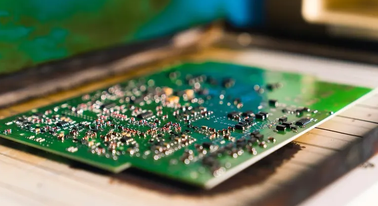
3. PCB Layout Fundamentals
The physical arrangement of components and traces significantly impacts your board’s performance and manufacturability.
3.1 Board Stackup Design
- Layer count: How many conductive layers does your design require? More layers add cost but can solve routing challenges.
- Material selection: Does your application require standard FR-4 or specialized materials (high-frequency, high-temperature, etc.)?
- Impedance control: Do any traces require controlled impedance? This affects layer arrangement and dielectric thicknesses.
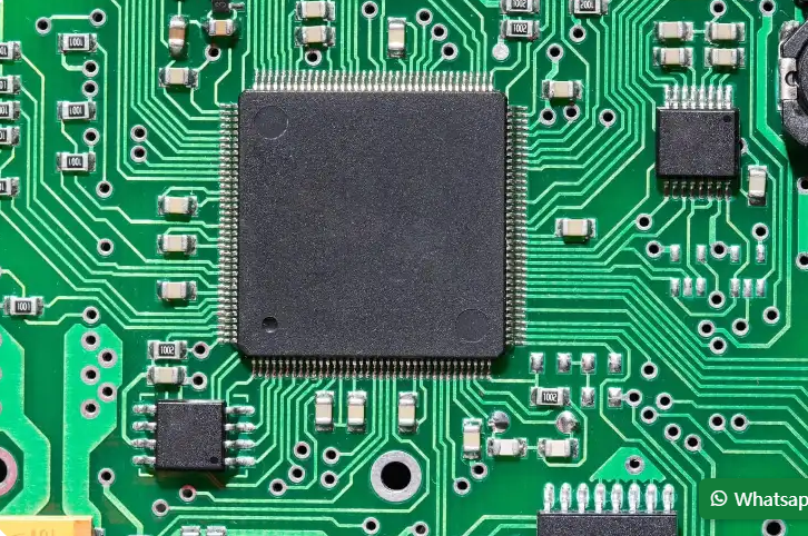
3.2 Component Placement
- Thermal considerations: Are heat-generating components properly positioned with adequate cooling provisions?
- Signal integrity: Are high-speed components placed to minimize critical path lengths?
- Manufacturing requirements: Does your placement allow for proper soldering (wave, reflow, or hand soldering)?
3.3 Routing Strategies
- Trace width: Have you calculated appropriate trace widths for expected current loads?
- Clearance rules: Are spacing requirements met for voltage differences between conductors?
- Routing priority: Which signals (power, ground, clocks, sensitive analog) should be routed first?
4. Power Distribution Network (PDN) Design
A robust power delivery system is essential for reliable circuit operation.
4.1 Power Plane Strategy
- Dedicated layers: Should power and ground have entire layers, or can they share space with signals?
- Split planes: How should different voltage domains be arranged on shared layers?
- Copper pour: Would ground pours on signal layers improve performance?
4.2 Decoupling
- Capacitor placement: Are decoupling capacitors positioned close to IC power pins?
- Value selection: Have you used appropriate combinations of bulk, ceramic, and tantalum capacitors?
- High-frequency bypassing: Does your design account for high-frequency power supply noise?
5. Signal Integrity Considerations
Maintaining signal quality becomes increasingly challenging with higher speeds and denser layouts.
5.1 High-Speed Design
- Transmission lines: Which signals require controlled impedance routing?
- Termination: Are appropriate termination schemes used for high-speed lines?
- Crosstalk: Have you implemented sufficient spacing or shielding between sensitive traces?
5.2 Mixed-Signal Design
- Grounding strategy: Should you use split grounds or a unified ground plane?
- Partitioning: Are analog and digital sections properly separated?
- Noise sensitive circuits: Are low-level analog signals protected from digital noise sources?
6. Thermal Management
Proper heat dissipation prevents premature failure and ensures reliable operation.
6.1 Heat Dissipation Techniques
- Copper areas: Can you use expanded copper features to conduct heat away from components?
- Thermal vias: Should you incorporate vias under hot components to transfer heat to other layers?
- Heatsinks: Does your design accommodate necessary heatsinks or other cooling methods?
6.2 Thermal Analysis
- Power dissipation: Have you calculated expected power dissipation for all components?
- Temperature rise: Will operating temperatures stay within component specifications?
- Airflow: If forced air cooling is needed, is component placement optimized for airflow?
7. Design for Manufacturing (DFM) Considerations
A design that can’t be reliably manufactured won’t succeed regardless of its electrical merits.
7.1 Fabrication Constraints
- Minimum feature sizes: Does your design respect the fabricator’s capabilities for trace width, spacing, and hole sizes?
- Annular rings: Are drilled holes properly centered in their pads?
- Silkscreen: Is component labeling clear and unobstructed?
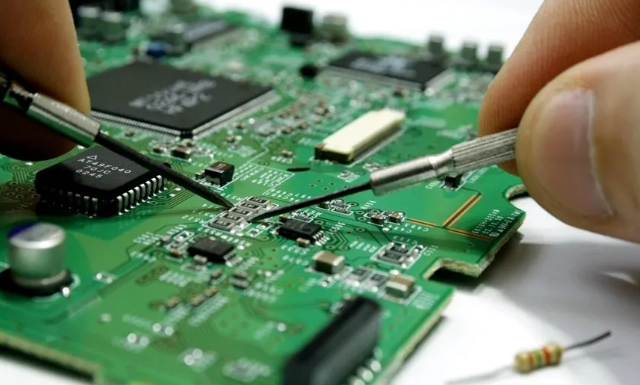
7.2 Assembly Considerations
- Component spacing: Is there adequate space for soldering and rework?
- Orientation: Are polarized components consistently oriented for automated assembly?
- Tool access: Can assembly tools reach all necessary locations?
8. Testing and Verification
Planning for testing during design can prevent headaches later.
8.1 Testability Features
- Test points: Have you included accessible test points for critical signals?
- Boundary scan: Does your design support JTAG or other test access methods?
- Probe access: Is there space for oscilloscope or logic analyzer probes?
8.2 Design Verification
- Design rule check (DRC): Have you run comprehensive DRC with appropriate rule settings?
- Electrical rule check (ERC): Does your netlist match intended connectivity?
- 3D visualization: Have you reviewed component clearances in three dimensions?
9. Documentation Requirements
Complete documentation ensures smooth transition to manufacturing and aids future modifications.
9.1 Manufacturing Files
- Gerber files: Are all necessary layers and features properly exported?
- Drill files: Do hole sizes and locations match your design?
- Assembly drawings: Are component locations and orientations clearly specified?
9.2 Bill of Materials (BOM)
- Complete parts list: Does your BOM include all components with correct designators?
- Procurement information: Are manufacturer part numbers and preferred suppliers identified?
- Alternates: Have you listed approved alternate components where applicable?
10. Iterative Improvement Process
PCB design is rarely perfect on the first attempt—plan for refinement.
10.1 Prototyping Strategy
- Test points: Have you included features to facilitate prototype debugging?
- Modification provisions: Can you easily cut traces or add jumper wires if needed?
- Diagnostic LEDs: Would status indicators help verify operation during testing?
10.2 Revision Control
- Version tracking: Do you have a system to manage design revisions?
- Change documentation: Are modifications properly recorded with reasons for changes?
- Archive practices: Are previous versions securely stored for reference?
Conclusion
Successful PCB design requires balancing multiple competing considerations—electrical performance, physical constraints, manufacturability, and cost. By systematically addressing each of the areas outlined above before beginning your layout, you can avoid common pitfalls and create designs that perform reliably in their intended applications. Remember that PCB design is an iterative process, and even experienced designers often go through multiple revisions to optimize their layouts. Investing time in thorough upfront planning will pay dividends throughout the product development cycle, resulting in higher quality boards that meet all requirements with minimal rework.