Placing DC/DC Regulators on PCB Backside to Free Up Space for Digital ICs on Frontside
Abstract
In modern PCB design, space optimization has become increasingly critical as electronic devices continue to shrink in size while incorporating more functionality. One effective strategy for maximizing board space is placing DC/DC switching regulators on the backside (bottom layer) of the PCB while keeping digital ICs on the frontside (top layer). This approach offers several advantages, including improved signal integrity, better thermal management, and more efficient use of board real estate. This article explores the benefits, design considerations, and best practices for implementing this technique in high-density PCB layouts.
1. Introduction
As electronic systems become more complex, PCB designers face the challenge of fitting more components into smaller spaces. Digital ICs, such as microcontrollers, FPGAs, and memory modules, often require clean power delivery and low-noise environments to function optimally. Meanwhile, DC/DC switching regulators—essential for converting input voltages to the required levels—can introduce electromagnetic interference (EMI) and thermal challenges.
By relocating DC/DC regulators to the backside of the PCB, designers can:
- Free up valuable space on the frontside for digital ICs and high-speed signal routing.
- Reduce noise coupling between switching regulators and sensitive analog/digital circuits.
- Improve thermal dissipation by leveraging the PCB as a heat spreader.
- Simplify power delivery network (PDN) design by minimizing loop inductance.
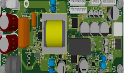
2. Benefits of Backside DC/DC Regulator Placement
2.1 Space Optimization
Modern PCBs, especially those in smartphones, IoT devices, and wearables, must accommodate numerous components in a limited area. Digital ICs often require more frontside space due to:
- High pin-count packages (e.g., BGA, QFN).
- Sensitive signal integrity requirements (e.g., DDR memory, high-speed serial links).
- The need for decoupling capacitors near power pins.
By moving DC/DC converters to the backside, designers can allocate more frontside space for digital ICs and their associated passive components.
2.2 Improved Signal Integrity
Switching regulators generate high-frequency noise due to their rapid switching transitions. Placing them on the backside helps by:
- Increasing physical separation from sensitive analog/digital traces.
- Reducing parasitic coupling through ground planes.
- Allowing better shielding through strategic use of ground fills.
2.3 Enhanced Thermal Performance
DC/DC regulators dissipate heat, which can affect nearby components. Backside placement offers thermal advantages:
- Heat can be dissipated through the PCB layers or into a metal chassis.
- Thermal vias can transfer heat away from critical frontside components.
- Separate thermal zones prevent digital ICs from overheating.
2.4 Simplified Power Delivery Network (PDN)
A well-designed PDN minimizes voltage drops and noise. Backside regulator placement helps by:
- Shortening high-current power paths to digital ICs.
- Reducing loop inductance through optimized via placement.
- Enabling better power plane segmentation.
3. Design Considerations for Backside DC/DC Placement
3.1 PCB Stackup and Layer Planning
A proper stackup is crucial for managing noise and heat. Recommended practices include:
- Using a solid ground plane between the frontside and backside to reduce noise coupling.
- Allocating dedicated power planes for different voltage domains.
- Ensuring sufficient copper thickness for high-current traces.
3.2 Thermal Management Techniques
- Thermal Vias: Place arrays of thermal vias under regulator ICs to conduct heat to inner layers or the opposite side.
- Copper Pours: Use large copper areas on the backside to spread heat.
- Heatsinks: Attach small heatsinks to backside regulators if needed.
3.3 EMI Mitigation Strategies
- Shielding: Use shielded inductors and cans to contain magnetic fields.
- Filtering: Add π-filters (LC networks) at regulator inputs/outputs.
- Grounding: Ensure low-impedance return paths for switching currents.
3.4 Component Placement and Routing
- Inductor Positioning: Keep inductors away from sensitive analog circuits.
- Minimizing Loop Area: Route high-current paths tightly to reduce EMI.
- Via Optimization: Use multiple vias for power connections to lower resistance and inductance.
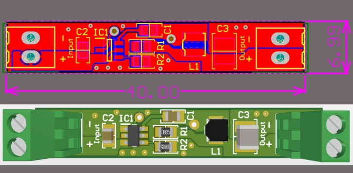
4. Case Study: Implementing Backside DC/DC in a High-Density Design
A wearable device PCB was redesigned to move two buck converters from the frontside to the backside. Results included:
- 20% more frontside space for the microcontroller and sensors.
- Reduced noise in analog sensor readings by 15%.
- Improved thermal performance, lowering the MCU’s operating temperature by 8°C.
5. Potential Challenges and Solutions
- Increased PCB Cost: More layers may be needed for proper isolation.
- Solution: Optimize layer count based on actual requirements.
- Assembly Complexity: Double-sided placement may require additional soldering steps.
- Solution: Use reflow-compatible components and proper stencil design.
- Thermal Crosstalk: Heat from backside regulators may affect frontside parts.
- Solution: Use thermal relief vias and copper balancing.
6. Conclusion
Placing DC/DC switching regulators on the backside of a PCB while keeping digital ICs on the frontside is a highly effective strategy for space-constrained designs. This approach enhances signal integrity, thermal performance, and power delivery efficiency. By following best practices in stackup design, thermal management, and EMI control, designers can achieve compact, high-performance layouts suitable for modern electronics.
Future trends, such as higher switching frequencies and advanced packaging techniques, will further drive the adoption of backside power placement in next-generation PCB designs.

