Why HASL (Hot Air Solder Leveling) is Not Recommended for High-Speed PCBs with Press-Fit Components
Introduction
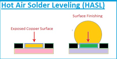
In the realm of high-speed printed circuit board (PCB) manufacturing, surface finish selection plays a critical role in determining the final product’s performance, reliability, and manufacturability. Among various surface finish options, Hot Air Solder Leveling (HASL), commonly referred to as solder coating or tin-lead/non-lead plating, has been a traditional choice for many years. However, when it comes to high-speed PCBs that incorporate press-fit components (also known as interference-fit or compliant-pin components), HASL presents numerous challenges that often make it unsuitable for these applications.
This article explores the technical reasons why HASL is generally not recommended for high-speed PCBs with press-fit components, examining issues related to mechanical integrity, signal integrity, thermal management, and long-term reliability.
Understanding Press-Fit Technology
Press-fit technology involves the insertion of component leads (typically pins) into plated through-holes on the PCB without using solder. The connection is maintained through mechanical interference between the pin and the hole wall. This technology offers several advantages:
- Elimination of solder-related defects (voids, cold joints, etc.)
- Suitable for high-temperature applications
- Allows for reworkability
- Provides reliable mechanical connection
Press-fit connections are commonly used in backplane applications, high-power systems, and high-speed digital applications where reliability under mechanical stress and thermal cycling is paramount.
The Challenges of HASL for Press-Fit Applications
1. Non-Uniform Surface Topography
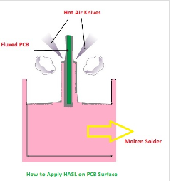
The HASL process involves dipping the PCB into molten solder and then using hot air knives to remove excess solder. This creates several problems for press-fit applications:
- Inconsistent hole fill: HASL often results in uneven solder deposition in plated through holes (PTHs), leading to variations in hole diameter. Press-fit pins require precise, consistent hole diameters to maintain proper interference fit.
- Solder bridging: Between closely spaced holes, HASL can create solder bridges that interfere with press-fit pin insertion.
- Solder protrusions: Irregular solder deposits around hole edges can prevent proper seating of press-fit components.
2. Dimensional Tolerance Issues
Press-fit technology relies on precise mechanical tolerances:
- Typical press-fit interference ranges from 0.05mm to 0.10mm
- HASL can add 0.025mm to 0.075mm of solder thickness unpredictably
- This variability can lead to:
- Excessive insertion force (damaging PCB or component)
- Insufficient retention force (poor electrical contact)
- Cracked barrel plating during insertion
3. Impact on High-Speed Signal Integrity
For high-speed PCBs (typically >1Gbps), HASL creates several signal integrity challenges:
- Surface roughness: HASL surfaces are relatively rough (Ra ≈ 1-3μm) compared to alternatives like ENIG (Ra ≈ 0.1-0.2μm), causing:
- Increased skin effect losses at high frequencies
- Impedance variations along transmission lines
- Greater insertion loss, especially above 5GHz
- Inconsistent thickness: Variations in HASL thickness (typically 1-25μm) create impedance mismatches that are particularly problematic for:
- Controlled impedance lines
- Differential pairs
- High-speed serial interfaces (PCIe, DDR, etc.)
- Solder meniscus: The curved solder surface at hole entries creates impedance discontinuities that can reflect high-speed signals.
4. Thermal Management Concerns
Press-fit components often handle significant power, and HASL exacerbates thermal issues:
- Thermal cycling reliability: The coefficient of thermal expansion (CTE) mismatch between HASL solder (Sn63Pb37 CTE ≈ 24ppm/°C) and PCB materials (FR4 CTE ≈ 14-17ppm/°C) creates stresses during temperature cycling that can:
- Crack barrel plating
- Degrade press-fit contact integrity
- Lead to intermittent connections
- Heat dissipation: The relatively low thermal conductivity of HASL solder (≈50W/mK) compared to copper (≈400W/mK) creates thermal barriers at critical interconnections.
5. Long-Term Reliability Issues
HASL presents several long-term reliability concerns for press-fit applications:
- Solder creep: Under constant mechanical stress from press-fit pins, HASL solder can undergo cold flow over time, reducing retention force.
- Intermetallic growth: At elevated temperatures, rapid growth of Cu-Sn intermetallics can occur at HASL interfaces, potentially embrittling connections.
- Oxidation: HASL surfaces oxidize over time, increasing contact resistance at press-fit interfaces where metal-to-metal contact is critical.
Alternative Surface Finishes for High-Speed PCBs with Press-Fit Components
Given these challenges, several alternative surface finishes are preferred for high-speed PCBs with press-fit components:
1. Electroless Nickel Immersion Gold (ENIG)
- Advantages:
- Flat, uniform surface ideal for press-fit
- Excellent high-frequency performance
- Good oxidation resistance
- Compatible with fine-pitch components
- Typical thickness: Ni 3-6μm, Au 0.05-0.1μm
2. Electroless Nickel Electroless Palladium Immersion Gold (ENEPIG)
- Advantages over ENIG:
- Better wire bondability
- Reduced “black pad” risk
- Superior corrosion resistance
- Typical thickness: Ni 3-6μm, Pd 0.1-0.3μm, Au 0.03-0.05μm
3. Organic Solderability Preservative (OSP)
- Advantages:
- Flat copper surface maintains precise hole dimensions
- Cost-effective
- Excellent for high-speed signals
- Considerations:
- Limited shelf life
- Not suitable for multiple reflow cycles
4. Immersion Silver (IAg)
- Advantages:
- Good high-frequency performance
- Flat surface topography
- Cost competitive
- Typical thickness: 0.2-0.4μm
5. Immersion Tin (ISn)
- Advantages:
- Flat surface
- Good solderability
- Cost effective
- Considerations:
- Potential for tin whiskers
- Limited shelf life
Process Considerations for Press-Fit Compatible Finishes
When selecting an alternative to HASL, manufacturers should consider:
- Hole wall quality: Ensure uniform plating distribution in PTHs
- Surface flatness: ≤10μm variation across the PCB
- Cleanliness: Remove all organic residues from hole walls
- Aging effects: Account for finish degradation over time
- Compatibility: Verify with component manufacturers’ specifications
Case Studies and Industry Trends
Industry data supports the migration away from HASL for high-speed press-fit applications:
- Telecommunications equipment: Major manufacturers report 30-50% reduction in intermittent connection failures by switching from HASL to ENIG for backplane press-fit connections.
- High-performance computing: PCIe Gen4 and Gen5 implementations show 0.5-1.5dB better insertion loss with ENIG compared to HASL at 16GHz.
- Automotive electronics: Press-fit connectors in engine control modules demonstrate 3× better thermal cycling performance with ENEPIG versus HASL.
Conclusion
While HASL remains a cost-effective surface finish for many conventional PCB applications, its limitations make it unsuitable for high-speed PCBs employing press-fit component technology. The combination of non-uniform surface topography, dimensional variability, signal integrity degradation, thermal management challenges, and long-term reliability concerns strongly suggests that alternative finishes like ENIG, ENEPIG, OSP, or immersion silver should be specified for these applications.
As data rates continue to increase and press-fit components find wider adoption in high-reliability applications, PCB designers and manufacturers must carefully evaluate surface finish options to ensure optimal performance and reliability. The additional cost of premium surface finishes is typically justified by reduced assembly defects, improved signal integrity, and enhanced product longevity in field operation.
By moving away from HASL for high-speed press-fit applications, electronics manufacturers can achieve:
- More reliable mechanical connections
- Better controlled impedance characteristics
- Improved thermal performance
- Higher yield in assembly
- Longer product service life
The industry trend clearly favors alternative finishes for these demanding applications, and designers are encouraged to specify these options early in the PCB fabrication process to avoid costly redesigns or field failures.