eDP Interface PCB Layout and Routing Guidelines
Introduction
Embedded DisplayPort (eDP) has become the dominant interface for connecting display panels to system boards in modern computing devices. As a high-speed digital interface derived from DisplayPort technology, eDP requires careful PCB design consideration to maintain signal integrity and ensure reliable operation. This article provides comprehensive guidelines for PCB layout and routing of eDP interfaces, covering key aspects such as stackup design, impedance control, routing topology, length matching, and EMI mitigation.
1. eDP Interface Overview
1.1 Basic Specifications
The eDP interface consists of:
- 1, 2, or 4 differential pairs for main link data (LANE0 to LANE3)
- Auxiliary channel (AUX CH) differential pair
- Hot Plug Detect (HDP) signal
- Panel power supply (PPWR) and backlight power
- Various control signals (PWM, ENABLE, etc.)
1.2 Speed Considerations
Current eDP versions support data rates up to 8.1 Gbps per lane (eDP 1.4b). Future versions will push this higher, making proper PCB design increasingly critical.
2. PCB Stackup Design
2.1 Recommended Stackup
For optimal eDP routing:
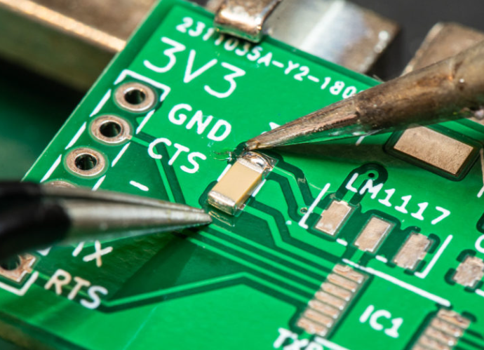
- Use at least 6-layer PCB for adequate reference planes
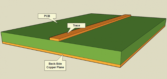
- Preferred stackup:
- Layer 1: Signal (microstrip)
- Layer 2: Ground plane
- Layer 3: Signal (stripline)
- Layer 4: Power plane
- Layer 5: Ground plane
- Layer 6: Signal (microstrip)
2.2 Dielectric Materials
Select low-loss dielectric materials (Dk ≈ 3.5-4.5, Df < 0.02 at 1 GHz) such as:
- FR408HR
- Isola 370HR
- Nelco N4000-13
3. Impedance Control
3.1 Differential Impedance Targets
- Main lanes: 100Ω differential (±10%)
- AUX channel: 90Ω differential (±10%)
3.2 Single-Ended Impedance
Maintain 50Ω single-ended impedance for all signals.
3.3 Impedance Calculation Factors
Consider:
- Trace width/spacing
- Dielectric thickness
- Copper thickness (typically 0.5 oz to 1 oz)
- Soldermask effects (can reduce impedance by 2-5Ω)
4. Routing Guidelines
4.1 General Routing Principles
- Route all differential pairs on the same layer when possible
- Maintain consistent spacing between pair members
- Avoid 90° bends – use 45° or curved traces
- Minimize via usage in high-speed paths
4.2 Trace Geometry
- Width/Spacing: 5/5 mil is typical for 100Ω diff pairs in standard FR4
- Keep spacing between pairs ≥ 3× the pair spacing
4.3 Length Matching Requirements
- Intra-pair skew: < 10 ps (≈ 15 mil at 6 Gbps)
- Inter-pair skew: < 100 ps (≈ 150 mil)
- AUX channel may have relaxed requirements
4.4 Layer Transitions
When vias are necessary:
- Use small diameter vias (8-10 mil drill)
- Place ground vias adjacent to signal vias
- Minimize stub length (back-drill if possible)
5. Power Delivery
5.1 Power Supply Routing
- Use wide traces for panel power (≥ 30 mil for 1A current)
- Implement proper decoupling:
- 10μF bulk capacitor near connector
- 0.1μF ceramic capacitor per power pin
5.2 Backlight Power
- Route as a guarded pair when PWM dimming is used
- Keep away from high-speed signals
- Consider separate ground return path
6. Grounding Strategy
6.1 Ground Plane Integrity
- Maintain unbroken ground reference under all high-speed traces
- Avoid splits or slots in reference planes
- Use multiple vias to connect ground layers
6.2 Ground Isolation
- Separate analog and digital grounds when needed
- Use single-point connection for different ground domains
7. EMI Mitigation
7.1 Shielding Techniques
- Use grounded copper pours around connectors
- Implement shield cans for sensitive areas
- Consider embedded shielding for critical applications
7.2 Filtering
- Add common-mode chokes on power lines if needed
- Use ferrite beads for low-frequency control signals
- Implement proper ESD protection at connectors
8. Connector Considerations
8.1 Connector Selection
- Choose connectors with impedance-matched contacts
- Prefer connectors with shielding features
- Verify mechanical robustness for the application
8.2 Connector Placement
- Position near edge for cable routing
- Provide adequate keep-out area for mechanical parts
- Ensure proper strain relief implementation
9. Design Verification
9.1 Signal Integrity Analysis
Perform simulations to verify:
- Eye diagram compliance
- Insertion loss
- Crosstalk levels
9.2 Design Rule Checking
Implement automated checks for:
- Impedance violations
- Length mismatches
- Spacing violations
10. Manufacturing Considerations
10.1 Tolerances
Account for manufacturing variations:
- ±1 mil trace width tolerance
- ±10% dielectric thickness variation
- ±0.5 mil etching variation
10.2 Testability
Include test points for:
- Power supply measurements
- Signal quality verification
- Protocol debugging
Conclusion
Proper PCB layout and routing of eDP interfaces requires attention to numerous details from stackup design to manufacturing considerations. By following these guidelines, designers can achieve reliable high-speed operation while meeting signal integrity and EMI requirements. As eDP data rates continue to increase, these practices will become even more critical for successful display implementations in modern electronic devices.

