PCB Design Considerations for FSPI (Flexible Serial Peripheral Interface)
Introduction
Flexible Serial Peripheral Interface (FSPI) is an emerging communication protocol that combines the advantages of traditional SPI with enhanced flexibility and performance characteristics. As electronic systems become more complex and demanding, FSPI has gained popularity in applications requiring high-speed data transfer, low power consumption, and configurable communication parameters. This article explores the critical PCB design considerations when implementing FSPI interfaces, covering layout techniques, signal integrity, power management, and design verification approaches.
Understanding FSPI Fundamentals
FSPI represents an evolution of the standard Serial Peripheral Interface (SPI), offering several improvements:
- Configurable data rates (often exceeding 100MHz)
- Flexible data frame formats
- Advanced error detection capabilities
- Lower power modes
- Enhanced signal integrity features
Unlike conventional SPI with fixed master-slave relationships, FSPI implementations often support dynamic role switching and more sophisticated topologies. These characteristics make proper PCB design crucial for achieving optimal performance.

Key PCB Design Considerations
1. Stackup and Material Selection
The foundation of any high-speed interface design begins with appropriate stackup configuration:
- Layer count: Minimum 4-layer board recommended (signal, ground, power, signal)
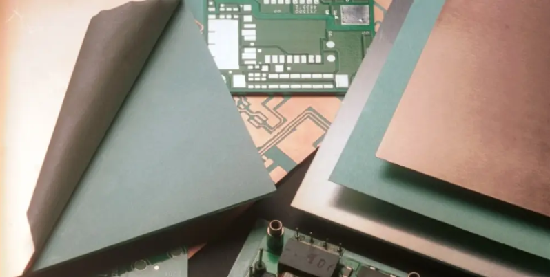
- Dielectric materials: Consider low-loss materials (Dk < 3.5, Df < 0.005) for high-speed applications
- Impedance control: Maintain consistent characteristic impedance (typically 50Ω single-ended, 100Ω differential)
- Layer arrangement: Place FSPI signals adjacent to solid reference planes
For designs operating above 50MHz, FR-4 may not provide sufficient performance, making high-frequency laminates like Rogers or Isola materials worth considering.
2. Signal Routing Techniques
Proper signal routing is paramount for FSPI interfaces:
Trace Geometry
- Maintain uniform trace width throughout the route
- Avoid 90° bends (use 45° angles or curved traces)
- Keep trace lengths matched (±50mil tolerance for clock/data pairs)
- Minimum spacing of 3× trace width between adjacent signals
Topology Management
- Point-to-point connections preferred for highest speeds
- For multi-drop configurations, use carefully designed stubs
- Consider fly-by topology for larger bus implementations
- Keep traces as short as possible (< 5″ for >50MHz operation)
Reference Planes
- Route over continuous reference planes (no splits)
- Avoid crossing plane gaps or changing reference layers
- Maintain at least 3× trace width clearance from plane edges
3. Clock Signal Integrity
The FSPI clock (SCLK) requires special attention:
- Implement length matching with data lines (±20mil recommended)
- Route clock signals first, with the most direct path
- Consider guard traces or ground shielding for sensitive clocks
- Avoid parallel routing with other high-speed signals
- Place series termination near the driver (typically 22-33Ω)
4. Power Delivery Network (PDN) Design
A robust PDN ensures stable FSPI operation:
- Use dedicated power planes or wide traces for FSPI power rails
- Implement proper decoupling (100nF + 1μF per power pin)
- Place decoupling capacitors close to IC power pins
- Consider power island techniques for sensitive analog supplies
- Maintain low impedance power paths (<0.1Ω target impedance)
5. Grounding Strategy
Effective grounding prevents noise issues:
- Use solid ground planes beneath FSPI signals
- Implement a unified ground system (avoid splits under FSPI)
- Place ground vias near connector shields and cable grounds
- Consider ground stitching vias along signal routes
- Maintain low inductance ground connections
6. Termination Techniques
Proper termination prevents reflections:
- Source termination (series resistors) for point-to-point
- Parallel termination may be needed for multi-drop
- AC termination for bidirectional signals
- On-die termination (ODT) if available
- Match termination values to trace impedance
7. Crosstalk Mitigation
Minimize interference between signals:
- Maintain 3H spacing rule (3× dielectric height between traces)
- Route orthogonal to potential aggressor signals
- Use ground guard traces for critical signals
- Consider differential routing for high-speed pairs
- Avoid long parallel runs with other high-speed interfaces
8. EMI Control
Reduce electromagnetic emissions:
- Implement proper return path continuity
- Use edge plating or shielding cans if needed
- Consider embedded stripline routing for sensitive signals
- Add ferrite beads or common-mode chokes as needed
- Follow 20H rule for plane edges
9. Connector and Interface Considerations
For board-to-board FSPI connections:
- Select connectors with proper bandwidth margin
- Match connector pinout to maintain signal integrity
- Consider impedance-controlled connectors
- Minimize stub lengths at connector interfaces
- Provide adequate grounding at connection points
10. Design for Manufacturing (DFM)
Ensure manufacturability:
- Follow manufacturer’s design rules for trace/space
- Provide proper solder mask clearance
- Include test points for critical signals
- Consider ICT access requirements
- Document special impedance requirements

Simulation and Verification
Pre-layout Simulation
- Perform signal integrity analysis for proposed stackup
- Model transmission line effects
- Simulate termination strategies
- Analyze power delivery network impedance
Post-layout Verification
- Conduct signal integrity checks (eye diagrams, timing)
- Verify power plane resonance modes
- Check for impedance discontinuities
- Validate timing margins
- Perform crosstalk analysis
Measurement Techniques
- Time-domain reflectometry (TDR) for impedance verification
- Vector network analyzer (VNA) for S-parameter measurement
- Oscilloscope analysis for signal quality
- Protocol analyzer for functional verification
Special Considerations for High-Speed FSPI
For implementations exceeding 100MHz:
- Consider microvia technology for dense designs
- Implement back-drilling for through-hole vias
- Use via-in-pad techniques for BGA devices
- Optimize solder mask application
- Specify controlled impedance for all interconnects
Thermal Management
High-speed FSPI operation may generate heat:
- Provide adequate copper for power dissipation
- Consider thermal vias under high-current devices
- Ensure proper airflow in enclosure
- Monitor temperature-sensitive components
Design Documentation
Complete documentation ensures successful manufacturing:
- Detailed stackup drawing with material specifications
- Impedance control requirements
- Special routing instructions
- Fabrication notes (surface finish, etc.)
- Assembly notes (component placement, etc.)

Conclusion
Designing PCBs for FSPI interfaces requires careful attention to signal integrity, power delivery, and layout techniques. By following these guidelines—proper stackup design, controlled impedance routing, effective termination, and thorough verification—designers can create robust FSPI implementations that meet performance requirements while maintaining signal quality. As FSPI continues to evolve with higher speeds and more advanced features, these PCB design considerations will become increasingly critical for successful product development.
Remember that each design presents unique challenges, and these guidelines should be adapted to specific application requirements. Collaboration with component manufacturers, PCB fabricators, and assembly partners early in the design process can help identify potential issues before they impact product performance or manufacturability.


