The Pros and Cons of Outer Layer Copper Pour in PCB Design
Introduction
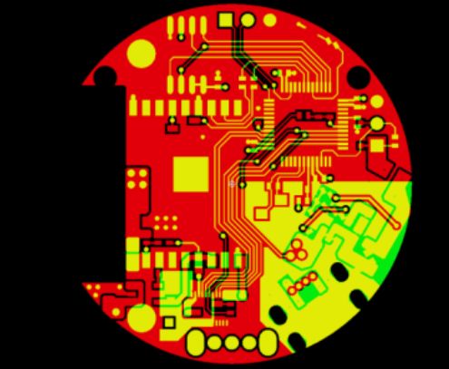
Printed Circuit Board (PCB) design involves numerous critical decisions that affect the board’s performance, manufacturability, and reliability. One such decision is whether to implement copper pour (also called copper flooding) on the outer layers of the PCB. Copper pour refers to the practice of filling unused areas of a PCB layer with solid copper that is typically connected to a ground network. This technique has become common in modern PCB design, but it presents both advantages and disadvantages that designers must carefully consider.
This article will examine in detail the benefits and drawbacks of implementing outer layer copper pour, covering electrical, thermal, mechanical, and manufacturing aspects. By understanding these factors, PCB designers can make informed decisions about when and how to use outer layer copper pour in their projects.
Benefits of Outer Layer Copper Pour
1. Improved Thermal Management
One of the primary advantages of outer layer copper pour is enhanced thermal performance:
Heat Dissipation: The copper on outer layers acts as a heat spreader, helping to dissipate heat from components. This is particularly valuable for power components or high-current traces that generate significant heat. The large copper areas provide additional thermal mass and surface area for heat transfer to the surrounding environment.
Thermal Relief for Components: Many surface-mount devices (SMDs) benefit from the thermal connection to copper pour, which helps maintain more stable operating temperatures. For components like power MOSFETs or voltage regulators, this can prevent overheating and improve reliability.
Reduced Thermal Stress: By providing more uniform temperature distribution across the board, copper pour can minimize thermal gradients that lead to mechanical stress during operation.
2. Enhanced Signal Integrity
Copper pour on outer layers can significantly impact the board’s electrical performance:
Controlled Impedance: For high-frequency designs, outer layer copper pour helps maintain consistent dielectric environments for transmission lines. This is crucial for impedance-controlled signals where the presence (or absence) of nearby copper affects the characteristic impedance.
Reduced Crosstalk: The copper pour acts as a shield between adjacent signal traces, minimizing electromagnetic interference (EMI) and crosstalk. This is especially important for dense layouts with many parallel traces carrying high-speed signals.
Improved Return Paths: When properly connected to ground, outer layer copper provides excellent return paths for high-frequency signals, reducing loop inductance and minimizing electromagnetic radiation.
3. EMI Reduction and Shielding
Radiated Emissions Control: A continuous copper pour on outer layers forms a partial Faraday cage that helps contain electromagnetic fields within the board. This reduces radiated emissions that could cause the product to fail electromagnetic compatibility (EMC) testing.
Susceptibility Protection: Conversely, the copper layer also provides some shielding against external electromagnetic interference that might affect circuit operation.
Edge Radiation Mitigation: When extended to the board edges (with proper connection to internal ground planes), outer layer copper can reduce edge radiation effects that often contribute to EMI problems.
4. Manufacturing Benefits
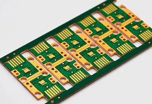
More Uniform Etching: Copper pour creates a more balanced copper distribution across the panel, which promotes uniform etching during manufacturing. This can lead to more consistent trace widths and better yield.
Reduced Board Warpage: The symmetrical copper distribution helps maintain board flatness by balancing the copper weight between layers. This is particularly important for large boards or those exposed to high temperatures during assembly.
Improved Solder Mask Application: A consistent copper surface provides better conditions for solder mask application compared to areas with drastic copper density variations.
5. Mechanical Strengthening
Increased Rigidity: The additional copper adds structural integrity to the PCB, making it less prone to flexing or bending. This can be important for large boards or those used in mechanically stressful environments.
Via Protection: Copper pour around vias can provide additional support, reducing the risk of via cracking due to thermal cycling or mechanical stress.
Drawbacks of Outer Layer Copper Pour
Despite its many advantages, outer layer copper pour also presents several potential disadvantages that must be considered:
1. Increased Risk of Solder Bridging
Solder Mask Challenges: Areas with copper pour near component pads may experience solder mask registration issues. If the solder mask doesn’t perfectly cover the copper, solder can wick away from pads during assembly, creating bridges or insufficient solder joints.
Tombstoning Risk: For small surface-mount components like resistors and capacitors, unequal copper distribution can create thermal imbalances during reflow that lead to tombstoning (one end lifting off the pad).
2. Potential for Ground Loops
Accidental Antennas: Poorly implemented copper pour can create ground loops that act as unintentional antennas, actually increasing EMI problems rather than reducing them.
Split Plane Issues: If the copper pour contains multiple isolated sections or is improperly connected to the ground system, it can cause more harm than good to signal integrity.
3. Manufacturing Complexity
Increased Etching Time: While uniform copper distribution helps etching consistency, the total amount of copper to be etched increases, potentially affecting production time and cost.
DFM Challenges: Designs with copper pour require careful attention to design-for-manufacturing (DFM) rules, including proper clearance from traces and pads, thermal relief connections, and copper balancing.
4. Rework Difficulties
Desoldering Challenges: The thermal mass of copper pour makes it more difficult to heat individual pads for component removal or rework.
Trace Access: Debugging and probing signals can be more challenging when they’re surrounded by copper pour, particularly if the pour isn’t properly segmented.
5. Potential for Corrosion
Exposed Copper: On outer layers, any breaks in the solder mask expose bare copper to the environment, which can lead to oxidation or corrosion over time unless special finishes are applied.
Electrochemical Migration: In humid environments, voltage differences across copper pour areas can lead to dendritic growth and eventual short circuits.
Best Practices for Implementing Outer Layer Copper Pour
To maximize the benefits while minimizing the drawbacks, consider these implementation guidelines:
- Proper Ground Connection: Ensure copper pour is correctly connected to the ground system with multiple vias to prevent antenna effects.
- Adequate Clearances: Maintain appropriate spacing between copper pour and signal traces (typically 2-3 times the trace width).
- Thermal Relief: Use thermal spokes for component connections to prevent soldering issues while maintaining electrical connection.
- Copper Balancing: Distribute copper evenly across layers to prevent warping, especially in multilayer boards.
- Segmentation: Consider dividing large copper areas with isolation gaps for high-frequency designs to prevent resonant structures.
- Solder Mask Coverage: Verify solder mask coverage over copper pour areas adjacent to component pads.
Conclusion
Outer layer copper pour is a powerful technique in PCB design that offers significant benefits in thermal management, signal integrity, EMI control, and manufacturability. However, these advantages come with potential drawbacks including soldering challenges, ground loop risks, and increased manufacturing complexity.
The decision to use outer layer copper pour should be based on the specific requirements of each design. High-frequency digital boards, RF circuits, and power electronics typically benefit greatly from well-implemented copper pour. Simpler, low-frequency designs might not require it and could avoid its potential downsides.
Ultimately, successful implementation requires careful attention to design rules, proper connection strategies, and consideration of manufacturing requirements. By understanding both the benefits and limitations of outer layer copper pour, PCB designers can make informed decisions that optimize the performance and reliability of their circuits while ensuring manufacturability and cost-effectiveness.