Optimization Methods for Densely Packed Solder Joints in PCB Design
Abstract
As electronic devices continue to shrink in size while increasing in functionality, printed circuit board (PCB) designs face significant challenges in managing densely packed solder joints. Overly dense solder joints can lead to manufacturing defects, reduced reliability, and signal integrity issues. This paper explores various optimization techniques for managing high-density solder joints in PCB design, including pad size adjustment, via optimization, solder mask application, component placement strategies, and advanced manufacturing considerations. By implementing these methods, designers can improve manufacturability, reliability, and performance in compact PCB layouts.
1. Introduction
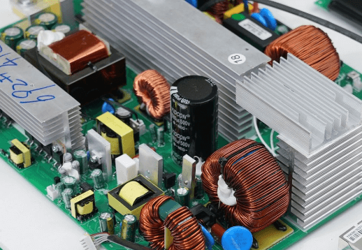
Modern PCB designs, especially in consumer electronics, IoT devices, and high-performance computing, demand increasingly dense component placement. This trend leads to closely spaced solder joints, which can cause several problems:
- Solder bridging: Unintended connections between adjacent pads due to excessive solder.
- Tombstoning: Uneven heating causing components (especially small passives) to lift on one side.
- Insufficient solder: Poor wetting or weak connections due to limited space.
- Thermal stress: Concentrated heat affecting joint reliability.
- Signal interference: Crosstalk between closely spaced traces.
To address these challenges, PCB designers must employ optimization techniques that balance density with manufacturability and reliability.

2. Pad Size and Shape Optimization
2.1 Reducing Pad Size While Maintaining Reliability
- Follow IPC-7351 standards for land pattern design.
- Use smaller pads for fine-pitch components (e.g., 0.4mm pitch QFNs).
- Ensure sufficient copper for mechanical strength but avoid excessive overlap.
2.2 Non-Standard Pad Shapes
- Oval or rectangular pads for fine-pitch ICs instead of circular ones.
- Home-plate shaped pads for QFN packages to improve solder flow.
- Elongated pads for passive components to prevent tombstoning.
2.3 Solder Mask Defined (SMD) vs. Non-Solder Mask Defined (NSMD) Pads
- SMD pads: Solder mask covers part of the pad, reducing bridging risk.
- NSMD pads: Better for BGA packages, allowing more solder volume.
3. Via Optimization in High-Density Areas
3.1 Microvia and Blind/Buried Via Technology
- Use laser-drilled microvias (≤0.1mm diameter) to save space.
- Implement blind and buried vias to reduce layer transitions.
3.2 Via-in-Pad Design
- Fill and plate vias in pads for BGAs and dense components.
- Requires plugging (conductive or non-conductive) to prevent solder wicking.
3.3 Via Tenting and Capping
- Cover unused vias with solder mask to prevent solder migration.
4. Solder Mask and Paste Application Techniques
4.1 Solder Mask Expansion and Clearance
- Tighten solder mask clearance (e.g., 0.05mm) to prevent bridging.
- Use liquid photoimageable solder mask (LPISM) for precise application.
4.2 Solder Paste Stencil Design
- Reduce aperture size for fine-pitch components (e.g., 80% pad area).
- Step stencils for mixed component sizes (thinner paste for small pads).
- Use nano-coated stencils for better paste release.
4.3 Solder Paste Selection
- Type 4 (20-38μm) or Type 5 (10-25μm) powder for fine features.
- Low-voiding pastes for high-reliability applications.
5. Component Placement and Routing Strategies
5.1 Optimal Component Orientation
- Align passive components in the same direction for even soldering.
- Rotate ICs to maximize spacing between adjacent pads.
5.2 Staggered Placement for BGAs and QFNs
- Alternate row/column spacing to reduce via congestion.
5.3 Trace Routing Between Pads
- Use thinner traces (e.g., 0.075mm) in dense areas.
- Escape routing in a radial pattern from BGAs.
6. Advanced Manufacturing and Design Techniques
6.1 Sequential Lamination for HDI PCBs
- Build up layers sequentially to accommodate dense interconnects.
6.2 Conductive Adhesives and Anisotropic Films
- Alternative to solder for ultra-fine pitch components.
6.3 Reflow Profile Optimization
- Ramp-soak-spike profiles to minimize tombstoning.
- Nitrogen reflow for better wetting in dense assemblies.
7. Design for Test (DFT) and Inspection
7.1 Automated Optical Inspection (AOI) Considerations
- Ensure adequate contrast between pads and solder mask.
- Include fiducials for alignment in dense layouts.
7.2 Test Point Accessibility
- Embed test points in via structures.
- Use boundary scan for high-density boards.
8. Conclusion
Optimizing densely packed solder joints in PCB design requires a multi-faceted approach, combining pad geometry adjustments, via management, solder mask control, and manufacturing-aware placement strategies. By implementing these techniques, designers can achieve higher component density without compromising reliability or manufacturability. Future advancements in materials, assembly processes, and design tools will further push the limits of miniaturization while maintaining robust solder joint integrity.