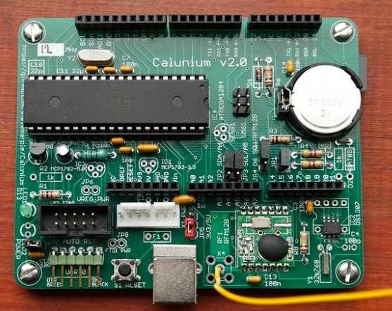
Overview of Modular Design Layout for PCB Modules
1. Introduction
Printed Circuit Board (PCB) design has evolved significantly with the increasing complexity of electronic systems. One of the most effective strategies to manage this complexity is modular design, where a PCB is divided into functional blocks or modules. This approach enhances reusability, simplifies debugging, and accelerates development cycles.
This article provides an in-depth overview of modular design layout techniques for PCB modules, covering key principles, partitioning strategies, signal integrity considerations, and best practices for implementation.

2. Principles of Modular PCB Design
Modular PCB design involves breaking down a circuit into independent functional blocks, each responsible for a specific task (e.g., power supply, microcontroller, RF communication). The key principles include:
2.1 Functional Partitioning
- Identify distinct functional blocks (e.g., power regulation, digital processing, analog signal conditioning).
- Define clear interfaces between modules to minimize cross-interference.
2.2 Reusability and Scalability
- Design modules to be reusable across different projects.
- Ensure standardized connectors and footprints for easy integration.
2.3 Signal and Power Integrity
- Isolate high-speed digital, analog, and RF sections to prevent noise coupling.
- Implement proper grounding strategies (e.g., split planes or star grounding).
2.4 Thermal Management
- Group high-power components together for efficient heat dissipation.
- Use thermal vias and heatsinks where necessary.
3. Layout Strategies for Modular PCBs
A well-planned layout is critical for modular PCB success. Below are key strategies:
3.1 Block-Based Placement
- Group related components (e.g., place all power supply components in one area).
- Minimize trace lengths between interconnected modules to reduce parasitic effects.
3.2 Hierarchical Routing
- Prioritize critical signals (e.g., high-speed clocks, differential pairs) with shortest paths.
- Use impedance-controlled routing for RF and high-speed digital signals.
3.3 Power Distribution Network (PDN) Optimization
- Decouple power supplies with localized capacitors near ICs.
- Avoid shared power paths between noise-sensitive and high-power modules.
3.4 Grounding Techniques
- Single-point grounding for analog circuits to prevent ground loops.
- Multi-ground plane separation for mixed-signal designs.

4. Signal Integrity Considerations
Modular PCBs must address signal integrity challenges:
4.1 Crosstalk Mitigation
- Increase spacing between parallel traces.
- Use guard traces or ground shielding for sensitive signals.
4.2 EMI Reduction
- Implement proper filtering (ferrite beads, LC filters).
- Enclose high-frequency modules with grounded shielding.
4.3 Controlled Impedance Routing
- Match trace widths to target impedance (e.g., 50Ω for RF, 90Ω for USB differential pairs).
- Avoid abrupt bends in high-speed signal paths.
5. Design for Manufacturing (DFM) and Testing
Modular PCBs should be designed for manufacturability and testability:
5.1 Standardized Footprints
- Use common component sizes to simplify assembly.
- Ensure module connectors are widely available.
5.2 Test Points and Debugging Access
- Include test pads for critical signals.
- Design modules for in-circuit testing (ICT) or boundary scan.
5.3 Panelization and Assembly
- Optimize module placement for automated pick-and-place machines.
- Consider depaneling methods (V-scoring, tab routing).
6. Case Study: Modular Design in IoT Devices
Many IoT devices use modular PCBs for flexibility. For example:
- Wireless Module: A pre-certified Bluetooth/Wi-Fi module simplifies RF design.
- Sensor Module: A separate analog front-end (AFE) ensures clean signal acquisition.
- Power Module: A buck/boost converter module provides stable voltage regulation.
By isolating these functions, designers can swap modules without redesigning the entire PCB.
7. Challenges and Solutions
7.1 Inter-Module Noise Coupling
- Solution: Use shielding cans or separate ground planes.
7.2 Connector Reliability
- Solution: Select high-quality connectors with sufficient mating cycles.
7.3 Thermal Crosstalk
- Solution: Position heat-generating modules away from temperature-sensitive components.

8. Future Trends in Modular PCB Design
- Embedded Modularity: System-in-Package (SiP) and chiplets for ultra-compact designs.
- AI-Assisted Layout: Machine learning for automated module placement and routing.
- Flexible PCBs: Stretchable modules for wearable electronics.
9. Conclusion
Modular PCB design enhances flexibility, reduces development time, and improves maintainability. By following structured partitioning, careful layout planning, and signal integrity best practices, engineers can create robust and scalable PCB modules. As electronics continue to evolve, modular design will remain a cornerstone of efficient PCB development.


