How to Avoid Crosstalk in PCB Design
Introduction
Crosstalk is a common issue in high-speed and high-density printed circuit board (PCB) designs, where unwanted electromagnetic coupling between adjacent signal traces causes interference. This phenomenon can lead to signal integrity problems, increased bit error rates, and even complete system failures. As modern electronics demand faster data rates and tighter PCB layouts, managing crosstalk has become increasingly critical.
This article explores the causes of crosstalk, its impact on PCB performance, and effective strategies to minimize it during the design phase.
1. Understanding Crosstalk in PCBs
1.1 What is Crosstalk?
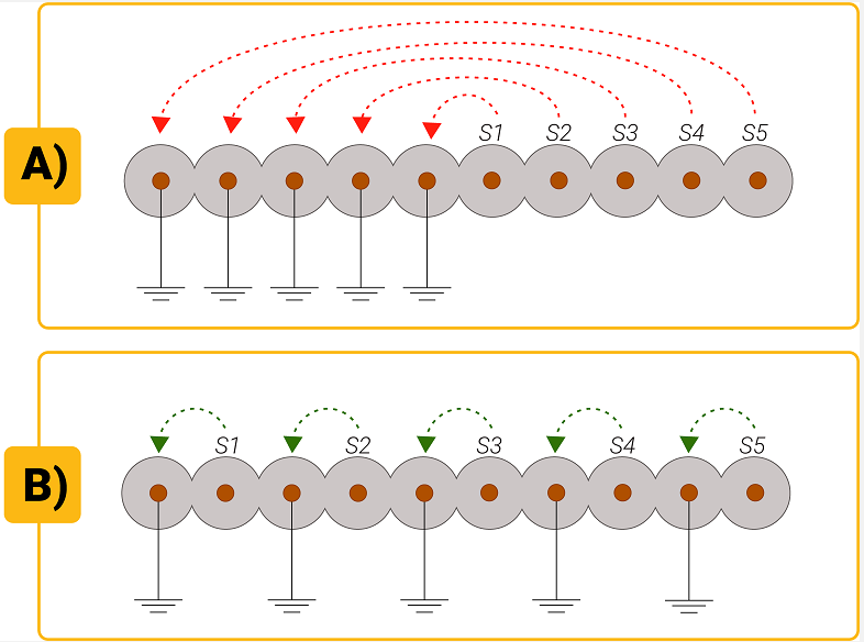
Crosstalk occurs when signals from one trace (the aggressor) induce unwanted noise in a nearby trace (the victim) through capacitive (electric field) or inductive (magnetic field) coupling. There are two primary types of crosstalk:
- Forward Crosstalk (Near-End Crosstalk – NEXT): Noise that travels in the same direction as the aggressor signal.
- Backward Crosstalk (Far-End Crosstalk – FEXT): Noise that propagates in the opposite direction of the aggressor signal.
1.2 Causes of Crosstalk
Several factors contribute to crosstalk in PCBs:
- High-Frequency Signals: Faster edge rates increase electromagnetic interference (EMI).
- Close Trace Proximity: Tightly spaced traces enhance coupling.
- Long Parallel Traces: Extended adjacent routing increases coupling effects.
- Impedance Mismatches: Poorly terminated traces reflect signals, worsening interference.
- Reference Plane Discontinuities: Inconsistent return paths increase crosstalk.
2. Key Strategies to Minimize Crosstalk
To mitigate crosstalk, PCB designers must follow best practices in layout, routing, and stackup design.
2.1 Proper Trace Spacing
The 3W Rule is a widely used guideline to minimize crosstalk:
- Keep adjacent traces at least three times the width of a trace (3W) apart.
For example, if a trace is 6 mils wide, spacing should be at least 18 mils to reduce coupling.
For high-speed designs, the 5W Rule (five times trace width) provides even better isolation.
2.2 Differential Pair Routing
Differential signaling (e.g., USB, PCIe, HDMI) helps reject common-mode noise. Key considerations:
- Maintain consistent spacing between the pair to ensure impedance matching.
- Route pairs symmetrically to avoid skew and phase differences.
- Avoid splitting pairs with vias or components, which can degrade signal integrity.
2.3 Controlled Impedance Design
- Use impedance calculators to determine trace width, spacing, and dielectric requirements.
- Match trace impedance to the source and load (e.g., 50Ω for single-ended, 100Ω for differential).
- Avoid abrupt changes in trace width, which cause reflections.
2.4 Ground and Power Planes
- Use solid reference planes (ground or power) beneath signal layers to provide a low-impedance return path.
- Avoid splits or gaps in reference planes under high-speed traces.
- Implement stitching vias near high-speed signals to maintain a continuous return path.
2.5 Minimize Parallel Trace Lengths
- Reduce parallel routing between sensitive signals.
- Route critical signals orthogonally (at 90° angles) to minimize coupling.
- Shorten long parallel runs by using meandering or serpentine routing only when necessary.
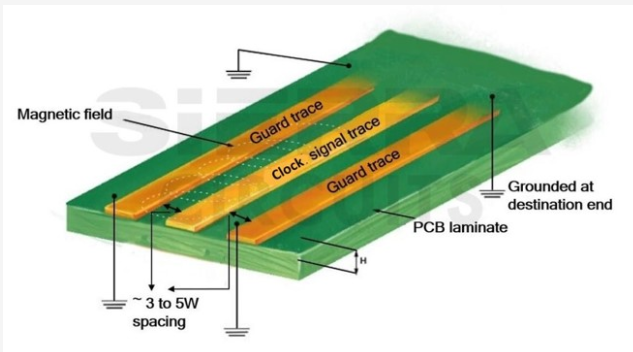
2.6 Shielding and Guard Traces
- Add ground guard traces between high-speed signals to block crosstalk.
- Use shielding (copper pours or grounded metal) around sensitive traces.
- Apply via fences (rows of grounding vias) to contain EMI.
2.7 Layer Stackup Optimization
- Separate high-speed signal layers with ground planes to reduce coupling.
- Avoid adjacent signal layers running in the same direction (prefer orthogonal routing).
- Use microstrip or stripline configurations for controlled impedance.
2.8 Termination Techniques
- Apply series termination (resistor at the source) to dampen reflections.
- Use parallel termination (resistor at the load) for impedance matching.
- Implement AC termination (RC networks) for high-frequency noise suppression.
2.9 Crosstalk Simulation and Analysis
- Use SI/PI (Signal Integrity/Power Integrity) tools like HyperLynx, Sigrity, or ADS to simulate crosstalk.
- Perform time-domain reflectometry (TDR) to detect impedance mismatches.
- Analyze S-parameters (S11, S21, NEXT, FEXT) in frequency-domain simulations.
3. Advanced Techniques for High-Speed Designs
3.1 Serpentine Routing for Length Matching
- Use controlled serpentine traces to match trace lengths without introducing excessive crosstalk.
- Keep meander spacing ≥ 3W to avoid self-coupling.
3.2 Embedded Passive Components
- Integrate resistors and capacitors into the PCB substrate to reduce parasitic effects.
- Minimize stub lengths to prevent signal reflections.
3.3 Backdrilling for Via Stubs
- Remove unused via portions (stubs) in high-speed signals (e.g., PCIe, DDR) to reduce resonance and crosstalk.
3.4 Low-Dk Dielectric Materials
- Choose low dielectric constant (Dk) materials (e.g., Rogers, Isola) to reduce capacitive coupling.
- Ensure consistent dielectric thickness to maintain impedance control.
4. Common Mistakes to Avoid
- Ignoring return current paths, leading to ground loops and increased crosstalk.
- Overlooking via transitions, which can introduce discontinuities.
- Using autorouters without constraints, resulting in poor signal integrity.
- Neglecting post-layout simulation, missing hidden crosstalk issues.
5. Conclusion
Crosstalk is a critical challenge in modern PCB design, especially with increasing signal speeds and density. By following best practices—such as proper trace spacing, impedance control, ground plane optimization, and simulation—designers can effectively minimize crosstalk and ensure robust signal integrity.
Advanced techniques like differential pair routing, shielding, and backdrilling further enhance performance in high-speed applications. A well-planned PCB stackup, combined with thorough signal integrity analysis, is essential for reducing crosstalk and achieving reliable electronic designs.
By implementing these strategies, engineers can mitigate crosstalk-related issues and improve the overall performance and reliability of their PCBs.