PCB Positive and Negative Film: Key Differences and Applications
Introduction to PCB Film Types
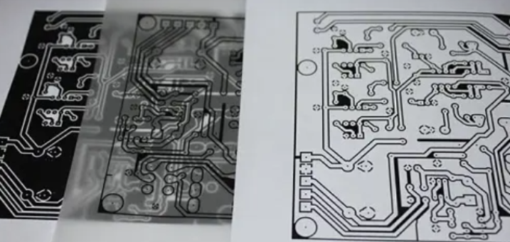
In printed circuit board (PCB) manufacturing, the terms “positive film” and “negative film” refer to two distinct approaches for transferring circuit patterns onto copper-clad boards. These photographic techniques serve as fundamental processes in PCB fabrication, each with unique characteristics that make them suitable for different applications. Understanding the difference between positive and negative film is essential for PCB designers and manufacturers to optimize their production processes and achieve desired circuit patterns efficiently.
Positive and negative films represent opposite approaches to pattern transfer. While they ultimately serve the same purpose—creating conductive pathways on PCBs—their working principles, advantages, and ideal use cases differ significantly. This article will explore these differences in detail, examining the technical aspects, manufacturing implications, and practical considerations for each method.
Understanding Positive Film in PCB Manufacturing
Positive film, also known as “positive photoresist” or “positive working film,” is a type of photomask where the circuit pattern appears as transparent areas on an opaque background. When exposed to light and developed, the exposed areas of the photoresist become soluble and are removed during development, leaving the unexposed areas to protect the underlying copper during etching.
The working principle of positive film follows these steps:
- The photoresist-coated copper board is exposed to UV light through the positive film mask
- Exposed areas of the photoresist undergo a chemical change, becoming soluble
- During development, the soluble photoresist is washed away, exposing the copper beneath
- The remaining photoresist protects the copper during etching
- After etching, all photoresist is removed, leaving only the desired copper traces
Key characteristics of positive film include:
- Clear areas on the film correspond to areas where copper will be removed
- The final copper pattern matches the opaque (black) areas of the film
- Generally provides better resolution for fine features
- Typically more expensive than negative film options
- Offers superior performance for complex, high-density designs
Positive film is particularly advantageous for designs requiring precise control over trace dimensions and spacing. The method tends to produce sharper edge definition, making it preferable for high-density interconnect (HDI) boards and designs with fine-pitch components. Many advanced PCB manufacturers prefer positive film for its ability to maintain consistent trace widths and spacing throughout the fabrication process.
Exploring Negative Film PCB Technology
Negative film, or “negative photoresist,” operates on the opposite principle from positive film. In this approach, the circuit pattern appears as opaque areas on a transparent background. When exposed to light, the unexposed areas (protected by the opaque pattern) remain after development, while the exposed areas become insoluble and remain on the board to protect the copper during etching.
The negative film process follows this sequence:
- The photoresist-coated board is exposed to UV light through the negative film mask
- Unexposed areas of the photoresist remain soluble while exposed areas harden
- Development removes the unexposed photoresist, exposing copper to be etched away
- The hardened photoresist protects desired copper traces during etching
- All remaining photoresist is stripped after etching completion
Distinctive features of negative film include:
- Opaque areas on the film correspond to copper traces that will remain
- The final copper pattern is the inverse of the film’s opaque pattern
- Generally more cost-effective than positive film processes
- Typically faster processing times
- Better suited for simpler designs with larger features
Negative film finds its strongest application in simpler PCB designs and mass production scenarios where cost efficiency is paramount. The process is generally more forgiving of exposure variations and can be more economical for large production runs. Many standard PCBs, especially those with larger features and less demanding tolerances, are produced using negative film techniques.
Comparative Analysis: Positive vs. Negative Film
When evaluating positive and negative film for PCB manufacturing, several key differences emerge that influence their suitability for various applications:
Resolution and Precision:
Positive film typically offers higher resolution capabilities, making it better suited for fine-pitch components and high-density designs. The process can reliably produce trace widths and spacings below 4 mils (0.1 mm), while negative film is generally limited to about 5 mils (0.127 mm) or larger features.
Cost Considerations:
Negative film processes are generally more economical, using less expensive materials and often requiring shorter processing times. Positive film, while more precise, involves higher material costs and more stringent process controls, resulting in increased production expenses.
Process Complexity:
Positive film requires more precise control of exposure times and development parameters. Negative film processes are somewhat more forgiving, making them easier to implement in less sophisticated manufacturing environments.
Yield and Defect Rates:
Positive film typically offers lower defect rates for complex designs due to its superior resolution capabilities. Negative film may have higher yield for simple designs but can struggle with more intricate patterns.
Material Compatibility:
Some advanced PCB materials respond better to one process over the other. High-frequency materials, for instance, often benefit from the precision of positive film processes.
Environmental Factors:
Negative film processes traditionally used more hazardous chemicals, though modern formulations have reduced this gap. Both methods now have relatively comparable environmental impacts with proper handling.
Production Volume:
Negative film shines in high-volume production of standard boards, while positive film is preferred for low-to-medium volume production of complex or high-performance boards.
Practical Applications and Selection Criteria
Choosing between positive and negative film depends largely on the specific requirements of the PCB being manufactured:
When to Use Positive Film:
- High-density interconnect (HDI) designs
- Boards with fine-pitch components (under 0.5 mm pitch)
- RF and microwave circuits requiring precise impedance control
- Multi-layer boards with complex interconnect requirements
- Designs with tight tolerances on trace width and spacing
- Advanced packaging applications
When Negative Film is Preferable:
- Simple single or double-sided boards
- Designs with larger features (traces/spaces > 5 mils)
- High-volume production where cost is critical
- Prototyping where quick turnaround is prioritized over precision
- Educational or hobbyist projects with less demanding requirements
Modern PCB fabrication often employs a hybrid approach, using positive film for critical layers and negative film for less demanding aspects of the board. This balanced method can optimize both cost and performance for many applications.
Technological Evolution and Future Trends
The distinction between positive and negative film processes continues to evolve with advancements in PCB technology:
Direct Imaging:
The growing adoption of laser direct imaging (LDI) systems is reducing reliance on physical films altogether. These systems project the circuit pattern directly onto the photoresist, offering the precision of positive processes with the flexibility of digital control.
Advanced Photoresists:
New photoresist formulations are blurring the lines between traditional positive and negative characteristics, with some materials offering the benefits of both approaches.
Additive Processes:
Emerging additive manufacturing techniques for PCBs may eventually reduce the need for subtractive etching processes altogether, potentially making the positive/negative film distinction obsolete for some applications.
Environmental Regulations:
Increasing environmental concerns are driving development of more eco-friendly photoresists and processing chemicals for both positive and negative methods.
Despite these advancements, the fundamental principles of positive and negative film remain relevant for understanding PCB fabrication processes and making informed design decisions.
Conclusion
The choice between PCB positive and negative film ultimately depends on the specific requirements of the circuit board being produced, balancing factors such as precision needs, cost constraints, and production volumes. Positive film offers superior resolution and precision for complex, high-density designs, while negative film provides a more cost-effective solution for simpler boards and high-volume production.
Understanding these differences enables PCB designers and manufacturers to select the most appropriate method for their specific application, optimizing both performance and manufacturing efficiency. As PCB technology continues to advance, the fundamental principles of these two approaches remain essential knowledge for anyone involved in electronic design and manufacturing.
While newer technologies like direct imaging are changing the landscape of PCB fabrication, the concepts underlying positive and negative film processes continue to inform the development of next-generation manufacturing techniques. By comprehending these traditional methods, engineers and manufacturers are better equipped to adopt and adapt to emerging technologies in the field of printed circuit board production.