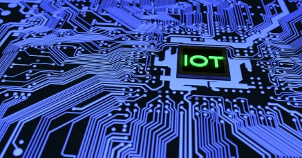
The Inseparable Connection Between Flexible/HDI PCBs and the Internet of Things (IoT)
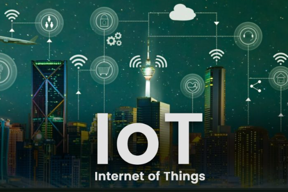
The Internet of Things (IoT) has emerged as one of the most transformative technological paradigms of the 21st century, connecting billions of devices into an intelligent, data-driven ecosystem. At the heart of this revolution lies advanced printed circuit board (PCB) technologies—specifically, flexible PCBs and high-density interconnect (HDI) PCBs—which enable the compact, reliable, and high-performance electronics required for IoT applications. From wearable fitness trackers to industrial sensors and smart home devices, flexible and HDI PCBs provide the essential foundation that makes IoT possible. This article explores why these PCB technologies are indispensable to IoT, examining their unique advantages, key applications, and future trends.
The Rise of IoT and Its Demands on PCB Technology
The IoT ecosystem is expanding at an unprecedented rate, with Gartner estimating over 26 billion connected devices by 2020, a number that has only grown since then . These devices span industries—consumer electronics, healthcare, automotive, industrial automation, and more—each requiring specialized PCB solutions to meet their operational demands. Traditional rigid PCBs, while sufficient for many conventional applications, often fall short in IoT environments where compactness, durability, and high-speed signal integrity are paramount.
IoT devices frequently operate in dynamic, space-constrained environments. Wearables must conform to the human body, industrial sensors endure harsh conditions, and smart home devices demand sleek, unobtrusive designs. Flexible and HDI PCBs address these challenges by offering:
- Miniaturization: IoT devices require dense component placement in small form factors.
- Durability: Many IoT applications involve movement, bending, or vibration.
- High-Speed Connectivity: IoT relies on seamless data transmission between devices and cloud platforms.
- Energy Efficiency: Battery-powered IoT devices need power-optimized circuitry.
These demands have propelled flexible and HDI PCBs to the forefront of IoT hardware development, making them inseparable from the IoT revolution.
Flexible PCBs: Enabling Compact and Durable IoT Devices
Flexible printed circuit boards (FPCBs) have become the go-to solution for IoT applications where traditional rigid boards cannot meet design requirements. Their unique properties make them ideal for the diverse and often challenging environments in which IoT devices operate.
Key Advantages of Flexible PCBs for IoT
- Compact Size and Flexibility
Most IoT devices feature striking contours and irregular shapes, requiring PCBs that can fit into tight, non-linear spaces. Flexible PCBs excel in this regard, as they can be folded into corners and conform to complex geometries without compromising performance. For instance, fitness trackers and smartwatches leverage flexible PCBs to achieve sleek, ergonomic designs that rigid boards could never accommodate . - Lightweight Construction
Flexible PCBs reduce device weight by up to 95% compared to traditional wiring harnesses, thanks to their ultra-thin substrates. This is critical for wearable IoT devices like hearing aids and medical sensors, where minimizing weight enhances user comfort and mobility . - Enhanced Reliability and Durability
IoT devices often endure mechanical stress—flexible PCBs can withstand millions of bending cycles without failure. Made from polyimide, these boards offer excellent thermal stability, resisting moisture, body heat, and constant motion, making them perfect for fitness trackers and industrial IoT sensors . - Simplified Wiring and Reduced Costs
Flexible PCBs eliminate bulky wire harnesses, reducing assembly complexity and costs associated with soldering and mechanical connectors. Their integrated interconnect systems also minimize wiring errors, enhancing manufacturing efficiency . - High-Density Design Capabilities
The thin substrates used in flexible PCBs allow for narrow traces, enabling more components per unit area—a crucial feature for IoT devices requiring sophisticated functionality in minimal space .
IoT Applications Leveraging Flexible PCBs
- Wearable Health Monitors: Devices like ECG patches and glucose monitors rely on flexible PCBs for comfort and continuous wearability.
- Smart Home Sensors: Motion detectors, smart locks, and environmental monitors use flexible circuits to fit into compact housings.
- Industrial IoT (IIoT): Vibration sensors and robotic actuators employ flexible PCBs to endure mechanical stress in harsh environments.
HDI PCBs: Powering High-Performance IoT Connectivity
While flexible PCBs address mechanical and spatial challenges, high-density interconnect (HDI) PCBs solve the signal integrity and miniaturization demands of advanced IoT systems. HDI technology enables finer traces, smaller vias, and higher component density, making it indispensable for high-speed, data-intensive IoT applications.
Key Advantages of HDI PCBs for IoT
- Dense Circuit Layouts
HDI PCBs utilize microvias, stacked vias, and fine-line traces to maximize routing density. This allows IoT devices to incorporate more functionality into smaller footprints—essential for smartphones, smartwatches, and medical implants . - Superior Electrical Performance
With shorter signal paths and reduced parasitic capacitance, HDI PCBs minimize signal loss and crosstalk. This is critical for IoT applications like 5G-enabled devices, where high-frequency data transmission is paramount . - Design Flexibility
HDI technology supports complex multilayer designs, enabling IoT manufacturers to integrate RF, power, and digital circuits efficiently. Advanced structures like “Any-layer HDI” allow direct connections between any two layers, further optimizing signal routing . - Improved Thermal Management
The close component placement in HDI PCBs reduces heat dissipation distances, enhancing thermal performance and prolonging device lifespan—an important consideration for always-on IoT nodes . - Cost Efficiency at Scale
Despite higher initial costs, HDI PCBs reduce overall system expenses by minimizing layer counts, improving yield rates, and enabling smaller form factors that save material costs .
IoT Applications Leveraging HDI PCBs
- AI-Enabled Edge Devices: Smart cameras and voice assistants use HDI PCBs to process data locally with minimal latency.
- Autonomous Sensors: Industrial condition-monitoring systems rely on HDI boards for reliable signal integrity in noisy environments.
- 5G IoT Modules: High-speed connectivity demands the precision routing and impedance control that only HDI technology can provide.
The Convergence of Flexible and HDI Technologies in IoT
Increasingly, IoT applications demand the combined benefits of flexible and HDI PCBs, leading to the rise of rigid-flex and advanced HDI-flex designs. These hybrid solutions offer:
- 3D Packaging Capabilities: Enabling ultra-compact IoT devices like foldable smartphones and implantable medical sensors.
- Enhanced Signal Integrity: Combining HDI’s high-speed routing with flexible interconnects reduces signal loss in dynamic environments.
- Improved Reliability: Rigid-flex constructions eliminate connector failure points, critical for automotive and aerospace IoT applications.
Companies like Samsung and Apple already utilize such technologies in their latest IoT-enabled devices, pushing the boundaries of what’s possible in consumer electronics .
Future Trends: How Flexible and HDI PCBs Will Shape Next-Gen IoT
As IoT continues evolving, flexible and HDI PCB technologies are advancing to meet emerging demands:
- Higher Density Interconnects
Next-generation HDI boards are pushing line widths below 30μm, enabling even more compact IoT devices with greater functionality . - Integration with Advanced Materials
New substrate materials like liquid crystal polymer (LCP) are enhancing flexible PCB performance in high-frequency 5G and millimeter-wave IoT applications. - 3D Printed Electronics
Additive manufacturing techniques promise to revolutionize flexible PCB production, enabling customized IoT solutions with faster turnaround times . - Sustainable PCB Solutions
Biodegradable flexible substrates and lead-free HDI processes are emerging to address environmental concerns in mass IoT deployments. - AI-Optimized Designs
Machine learning is being applied to optimize HDI routing and flexible PCB layouts for maximum performance in specific IoT use cases .
Conclusion: An Inseparable Partnership
Flexible and HDI PCBs have become foundational technologies for the IoT revolution, each addressing critical challenges that traditional PCBs cannot solve. Flexible PCBs provide the mechanical adaptability needed for wearable and compact IoT devices, while HDI technology delivers the signal integrity and component density required for high-performance applications. Together, they enable the sophisticated, reliable, and miniaturized electronics that make IoT possible across industries.
As IoT continues penetrating every aspect of modern life—from smart cities to personalized healthcare—the importance of advanced PCB technologies will only grow. Manufacturers who master flexible and HDI PCB design will lead the next wave of IoT innovation, shaping a future where billions of connected devices work seamlessly to transform how we live, work, and interact with our world. The bond between these PCB technologies and IoT is not just strong—it’s fundamentally inseparable, driving progress in both fields for years to come.