Can PCB Winding Technology Reshape Transformer and Inductor Design?
Abstract
This paper explores the transformative potential of Printed Circuit Board (PCB) winding technology in the design and manufacturing of transformers and inductors. As power electronics continue to evolve toward higher efficiency, smaller form factors, and greater reliability, PCB winding emerges as a promising alternative to traditional wire-wound components. The article examines the technical advantages, manufacturing benefits, performance characteristics, and current limitations of PCB-based magnetics. Through analysis of recent developments and case studies, we evaluate whether this technology can fundamentally reshape the landscape of transformer and inductor design across various applications including power supplies, electric vehicles, and renewable energy systems.
Introduction
The fundamental principles of transformer and inductor design have remained largely unchanged for over a century, with copper wire wound around magnetic cores forming the basis of these essential components. However, the emergence of PCB winding technology challenges this traditional paradigm by offering an alternative manufacturing approach that aligns with modern electronic production methods.
PCB winding technology involves creating conductive traces on one or multiple PCB layers to form the winding structures of transformers and inductors. This approach leverages standard PCB manufacturing processes to produce magnetic components with precise geometric control, excellent repeatability, and potential integration with other circuit elements.
As power electronics push toward higher frequencies, greater power densities, and more compact designs, the limitations of conventional wire winding—including labor-intensive manufacturing, inconsistent quality, and thermal management challenges—have become increasingly apparent. PCB winding technology promises to address many of these limitations while introducing new possibilities in component design.
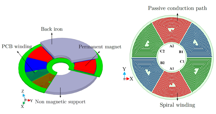
Technical Advantages of PCB Winding
Precision and Consistency
PCB manufacturing offers exceptional precision in trace geometry, enabling winding designs with tight tolerances that are difficult to achieve with conventional wire winding. This precision translates to:
- Consistent electrical parameters (inductance, resistance, capacitance)
- Repeatable performance across production batches
- Accurate control over turn ratios and leakage inductance
- Elimination of manual winding variations
Thermal Management
The planar nature of PCB windings provides inherent thermal advantages:
- Large surface area for heat dissipation
- Direct thermal paths to heatsinks or chassis
- Opportunity for embedded thermal vias and heat spreading layers
- Even distribution of thermal stresses
High-Frequency Performance
PCB windings demonstrate superior characteristics at high frequencies:
- Controlled parasitic capacitance through precise layer spacing
- Reduced proximity and skin effects through optimized trace geometries
- Better high-frequency resistance (Rac) characteristics
- Improved impedance matching at RF frequencies
Integration Capabilities
PCB technology enables unprecedented integration possibilities:
- Embedding of magnetic components within multilayer boards
- Co-fabrication with control circuitry
- Precise alignment between primary and secondary windings
- Integration of sensing elements for monitoring
Manufacturing Benefits
Scalability and Automation
PCB winding leverages existing PCB manufacturing infrastructure:
- Fully automated production processes
- High-volume manufacturing capability
- Elimination of manual winding labor
- Consistent quality control through visual and electrical testing
Design Flexibility
PCB technology offers new degrees of design freedom:
- Arbitrary winding shapes beyond circular forms
- Precise control over turn spacing and layer arrangements
- Easy implementation of interleaved windings
- Customizable terminal configurations
Material Options
PCB construction allows material optimization:
- Choice of dielectric materials with specific properties
- Flexible PCB substrates for unconventional form factors
- High-temperature materials for demanding applications
- Specialized copper weights and finishes
Performance Characteristics and Limitations
Electrical Performance
PCB windings exhibit distinct electrical characteristics:
- Typically lower fill factors compared to round wire
- Higher DC resistance for equivalent cross-sections
- More controllable interwinding capacitance
- Different leakage inductance profiles
Power Density Considerations
The tradeoffs in power density:
- Lower copper utilization in single-layer implementations
- Improved utilization through multilayer designs
- Compromise between conduction losses and size
- Opportunities for 3D integration to recover density
High-Current Limitations
Challenges in high-current applications:
- Current carrying capacity limited by trace width and copper weight
- Thermal limitations of PCB materials
- Solutions involving parallel traces and thermal management
High-Voltage Constraints
Considerations for high-voltage isolation:
- Creepage and clearance requirements
- Dielectric strength of PCB materials
- Techniques for enhanced isolation in PCB designs
Applications and Case Studies
Switch-Mode Power Supplies
PCB transformers in power conversion:
- Isolated DC-DC converters
- Gate drive transformers
- High-frequency resonant converters
- Point-of-load applications
Automotive Electronics
Transformative potential in electric vehicles:
- On-board chargers
- DC-DC converters
- Traction inverters
- Meeting automotive reliability standards
Renewable Energy Systems
Applications in sustainable energy:
- Solar microinverters
- Wind power converters
- Energy storage systems
- High-voltage applications
Telecommunications
RF and signal applications:
- Broadband transformers
- Impedance matching networks
- Miniaturized RF inductors
- High-frequency power combiners
Future Developments and Research Directions
Advanced Materials
Emerging materials for enhanced performance:
- High-temperature substrates
- Thermally conductive dielectrics
- Alternative conductive materials
- Nanocomposite magnetic materials
3D Integration
Innovations in three-dimensional structures:
- Embedded magnetic components
- Hybrid wire-PCB combinations
- Additive manufacturing approaches
- Vertical interconnection techniques
Design Tools and Optimization
Advances in modeling and simulation:
- Multiphysics simulation platforms
- AI-assisted design optimization
- Automated design rule checking
- Integrated thermal-electromagnetic modeling
Standardization Efforts
Industry-wide adoption challenges:
- Development of design standards
- Reliability testing protocols
- Performance benchmarking
- Industry consortium activities
Conclusion
PCB winding technology presents a compelling alternative to traditional wire-wound magnetics, offering significant advantages in precision, repeatability, thermal management, and integration potential. While the technology currently faces limitations in very high-current and high-voltage applications, ongoing advancements in materials, manufacturing techniques, and design methodologies are rapidly expanding its viable operating range.
The ability to produce transformers and inductors using standard PCB manufacturing processes represents more than just an incremental improvement—it offers the potential to fundamentally reshape magnetic component design. By enabling tighter integration, better performance predictability, and new form factors, PCB winding technology could drive innovation across numerous power electronics applications.
As research continues to address current limitations and industry adoption grows, PCB-based magnetics may well become the dominant paradigm for many transformer and inductor applications, particularly in space-constrained, high-frequency, or high-reliability scenarios. While traditional wire-wound components will likely maintain certain niches, the future of magnetic component design appears increasingly planar.
The question is not whether PCB winding technology will impact transformer and inductor design, but rather how profoundly and how quickly this transformation will occur across different segments of the power electronics industry. What remains certain is that designers now have a powerful new tool in their arsenal for meeting the ever-growing demands of modern electronic systems.