Analysis of Factors Leading to PCB Warpage
Abstract
Printed Circuit Board (PCB) warpage is a critical quality issue in electronics manufacturing that can lead to assembly defects, reliability problems, and functional failures. This paper comprehensively analyzes the various factors contributing to PCB deformation, including material properties, design characteristics, manufacturing processes, and environmental conditions. Through systematic examination of these influencing elements, we provide insights into warpage mechanisms and offer recommendations for prevention and control. The analysis draws upon industry standards, experimental data, and manufacturing experience to present a holistic view of PCB warpage causes and potential mitigation strategies.
1. Introduction
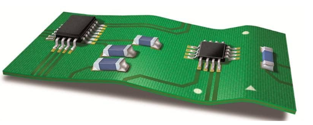
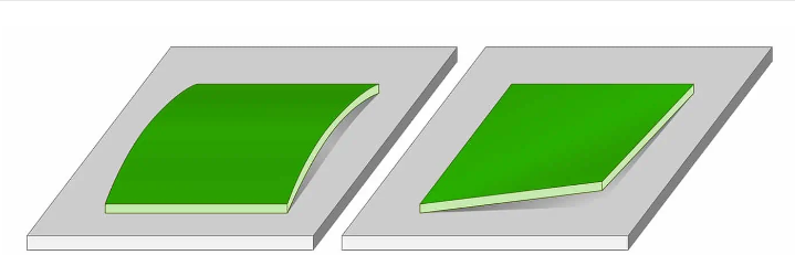
PCB warpage refers to the undesired bending or twisting of circuit boards that deviates from their intended flatness. In modern electronics manufacturing where component miniaturization and high-density interconnects are prevalent, even minor board deformation can cause significant problems. Warpage affects solder joint quality during surface mount technology (SMT) processes, creates mechanical stress on components, and may ultimately lead to field failures.
The increasing complexity of PCB designs, combined with demanding application environments, has made warpage control more challenging than ever. This paper categorizes and examines the multifactorial causes of PCB deformation, providing manufacturers and designers with a framework for understanding and addressing this persistent issue.
2. Material-Related Factors
2.1 Copper Layer Distribution
The asymmetric distribution of copper layers is one of the primary causes of PCB warpage. Copper and dielectric materials have different coefficients of thermal expansion (CTE). During thermal cycles in manufacturing, uneven copper distribution creates imbalanced stresses:
- Inner Layer Imbalance: Non-uniform copper coverage between layers (e.g., 70% on one layer vs. 30% on the opposite layer) creates tension differentials
- Copper Thickness Variations: Inconsistent copper weights (e.g., 1 oz vs. 2 oz) across layers exacerbates the imbalance
- Pattern Density Differences: High-density routing areas vs. large copper pours create localized stress concentrations
2.2 Core Material Properties
The dielectric materials used in PCB cores significantly influence warpage characteristics:
- CTE Mismatch: The Z-axis CTE of FR-4 (typically 50-70 ppm/°C) differs substantially from copper (17 ppm/°C)
- Tg (Glass Transition Temperature): High-Tg materials (170°C+) generally show better dimensional stability but may require higher lamination temperatures
- Resin Content: Higher resin percentages typically reduce stiffness and increase warpage susceptibility
- Prepreg Type: Different glass weave styles (1080, 2116, etc.) affect mechanical stability
2.3 Material Moisture Absorption
PCB materials absorb moisture from the environment, which can lead to swelling and subsequent warpage during high-temperature processes:
- Exposure to high-humidity environments before lamination
- Inadequate baking of materials prior to assembly
- Hygroscopic nature of certain resin systems
3. Design-Related Factors
3.1 Layer Stackup Configuration
The arrangement of layers and materials profoundly affects warpage:
- Symmetry Principle Violations: Asymmetric stackups (odd layer counts without balancing) increase warpage risk
- Core/Prepreg Thickness Variations: Inconsistent dielectric thickness between layers creates stress imbalances
- Mixed Material Construction: Combining different material types (e.g., FR-4 with polyimide) without proper transition
3.2 Board Geometry
Physical board characteristics influence deformation tendencies:
- Aspect Ratio: Length-to-width ratios exceeding 3:1 increase warpage susceptibility
- Board Thickness: Thin boards (<0.8mm) are more prone to warpage than thicker ones
- Cutouts and Irregular Shapes: Internal cutouts and complex contours create stress concentration points
3.3 Copper Balancing
Strategic copper distribution helps minimize warpage:
- Copper Thieving: Adding non-functional copper in sparse areas to balance density
- Hatch Patterns: Using cross-hatched copper instead of solid pours in large areas
- Layer-to-Layer Mirroring: Matching copper distribution patterns on opposing layers
4. Manufacturing Process Factors
4.1 Lamination Process
The multilayer pressing operation significantly impacts final board flatness:
- Temperature Profile: Uneven heating or excessive ramp rates create internal stresses
- Pressure Distribution: Non-uniform press plate contact causes localized deformation
- Cooling Rate: Rapid cooling after lamination “freezes in” residual stresses
4.2 Thermal Processing
Multiple high-temperature processes contribute to cumulative warpage:
- Solder Mask Curing: Typically involves multiple heating cycles (140-160°C)
- Hot Air Solder Leveling (HASL): Exposes boards to 260°C+ temperatures
- Baking Operations: Improper drying cycles can induce additional stresses
4.3 Mechanical Processing
Physical handling and machining operations affect board flatness:
- Routing/V-Scoring: Cutting operations release internal stresses unevenly
- Depanelization Methods: Punching vs. routing creates different stress patterns
- Handling Stress: Improper board support during transportation and storage
5. Environmental Factors
5.1 Temperature Cycling
Operational thermal cycles cause progressive warpage:
- Repeated expansion/contraction of dissimilar materials
- Stress relaxation over multiple cycles
- Creep deformation at elevated temperatures
5.2 Humidity Effects
Moisture-related dimensional changes:
- Hygroscopic expansion of dielectric materials
- Swelling-induced stress at copper/dielectric interfaces
- Accelerated aging in humid environments
5.3 Storage Conditions
Improper storage exacerbates warpage issues:
- Exposure to high humidity without protective packaging
- Stacking boards without proper support
- Long-term storage under stress
6. Warpage Measurement and Standards
6.1 Measurement Methods
Common techniques for quantifying warpage:
- Shadow Moiré: Optical measurement of surface contours
- Laser Scanning: Non-contact 3D surface profiling
- Contact Profilometry: Mechanical measurement of surface variations
6.2 Industry Standards
Relevant specifications for PCB flatness:
- IPC-6012: Defines maximum allowable warpage (typically 0.75-1.5%)
- IPC-TM-650: Standard test methods for warpage measurement
- J-STD-003: Solderability tests accounting for board warpage
7. Mitigation Strategies
7.1 Design Optimization
- Implement symmetrical layer stackups with balanced copper
- Use warpage simulation tools during design phase
- Incorporate stiffeners or balanced copper in critical areas
7.2 Material Selection
- Choose materials with matched CTE characteristics
- Consider low-CTE or high-Tg materials for demanding applications
- Evaluate moisture-resistant dielectric systems
7.3 Process Controls
- Optimize lamination temperature/pressure profiles
- Implement controlled cooling processes
- Establish proper handling and storage protocols
7.4 Post-Manufacturing Corrections
- Thermal flattening processes (with proper fixturing)
- Mechanical flattening for mild warpage cases
- Selective stress relief through targeted heating
8. Conclusion
PCB warpage results from complex interactions between material properties, design choices, manufacturing processes, and environmental conditions. Effective warpage control requires a holistic approach addressing all contributing factors throughout the product lifecycle. By understanding these mechanisms and implementing appropriate prevention strategies, manufacturers can significantly reduce warpage-related defects and improve product reliability.
Future developments in material science, simulation technologies, and process controls will continue to advance warpage management capabilities. However, the fundamental principles of balanced design, material compatibility, and process optimization remain essential for minimizing PCB deformation in electronic assemblies.