Key Considerations in PCB Manufacturing: A Comprehensive Guide
Printed Circuit Board (PCB) manufacturing is a complex process that requires careful attention to detail at every stage. Whether you’re an electronics designer, engineer, or manufacturer, understanding the critical aspects of PCB fabrication can mean the difference between a high-quality, reliable product and one that fails prematurely. This article explores the essential considerations in PCB manufacturing, covering design, material selection, fabrication processes, quality control, and emerging trends.
1. Design Considerations
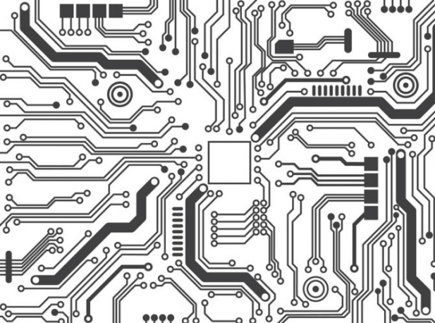
1.1 Proper Layout and Routing
The foundation of a successful PCB begins with proper design:
- Trace width and spacing: Ensure adequate trace widths for current carrying capacity and proper spacing to prevent short circuits and crosstalk
- Component placement: Optimize component placement for thermal management, signal integrity, and manufacturability
- Layer stackup: Carefully plan layer arrangement for multilayer boards to minimize interference and ensure proper impedance control
- Design for Manufacturability (DFM): Follow manufacturer’s guidelines for minimum trace widths, hole sizes, and spacing requirements
1.2 Signal Integrity and EMI Considerations
- Implement proper grounding techniques (star grounding, ground planes)
- Use appropriate trace routing for high-speed signals (length matching, differential pairs)
- Consider electromagnetic compatibility (EMC) requirements early in the design
1.3 Thermal Management
- Incorporate adequate thermal relief for components
- Plan for heat dissipation through proper copper distribution
- Consider thermal vias for heat transfer in multilayer boards
2. Material Selection
2.1 Substrate Materials
Choosing the right substrate material is crucial for PCB performance:
- FR-4: Standard material for most applications, good mechanical and electrical properties
- High-frequency materials: (Rogers, Teflon) for RF and microwave applications
- High-Tg materials: For applications requiring higher temperature resistance
- Flexible materials: (Polyimide) for flexible PCBs
2.2 Copper Foil
- Consider copper weight (typically 1oz/ft² or 2oz/ft²) based on current requirements
- Electrodeposited (ED) vs. rolled copper for different applications
2.3 Surface Finishes
Select appropriate surface finish based on application requirements:
- HASL (Hot Air Solder Leveling): Cost-effective but not suitable for fine-pitch components
- ENIG (Electroless Nickel Immersion Gold): Good for fine-pitch components and wire bonding
- OSP (Organic Solderability Preservative): Economical but limited shelf life
- Immersion Silver/Tin: Alternative finishes with specific advantages
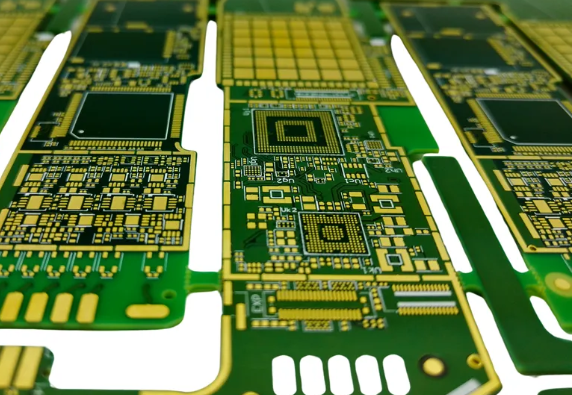
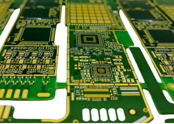
3. Fabrication Process Considerations
3.1 Imaging and Etching
- Ensure proper photoresist application and exposure for accurate pattern transfer
- Control etching process to maintain trace width integrity
- Monitor etch factor (ratio of vertical to horizontal etching)
3.2 Drilling
- Select appropriate drill bits for hole size and material
- Consider aspect ratio (board thickness to hole diameter) limitations
- Manage drill wear to maintain hole quality
3.3 Plating
- Ensure uniform copper plating in through-holes
- Monitor plating thickness for reliability
- Address potential plating voids or defects
3.4 Solder Mask Application
- Select appropriate solder mask type (LPI, dry film)
- Ensure proper registration and curing
- Consider solder mask dam requirements for fine-pitch components
3.5 Surface Finish Application
- Control thickness and uniformity of surface finish
- Prevent oxidation and contamination
- Consider shelf life implications of chosen finish
4. Quality Control and Testing
4.1 Electrical Testing
- Implement 100% electrical testing (flying probe or fixture testing)
- Verify netlist continuity and isolation
- Test for short circuits and open circuits
4.2 Visual Inspection
- Automated Optical Inspection (AOI) for surface defects
- Manual inspection for critical areas
- Verify solder mask and legend quality
4.3 Dimensional Verification
- Check board dimensions and hole sizes
- Verify registration of layers in multilayer boards
- Confirm impedance control where required
4.4 Reliability Testing
- Thermal cycling tests
- Solderability tests
- Environmental stress testing (humidity, chemical resistance)
5. Special Considerations for Different PCB Types
5.1 Multilayer Boards
- Careful layer alignment and registration
- Proper via design (through-hole, blind, buried)
- Impedance control for critical signals
- Lamination process control
5.2 High-Density Interconnect (HDI) PCBs
- Microvia formation and reliability
- Sequential lamination processes
- Fine line trace and space requirements
- Advanced materials for improved performance
5.3 Flexible and Rigid-Flex PCBs
- Material handling during fabrication
- Bend radius considerations
- Adhesive selection and application
- Coverlay application and registration
6. Environmental and Regulatory Compliance
6.1 RoHS Compliance
- Ensure materials and processes comply with RoHS directives
- Proper documentation of material content
- Lead-free manufacturing processes
6.2 Waste Management
- Proper handling and disposal of chemical wastes
- Recycling of copper and other materials
- Water treatment and conservation
6.3 Industry Standards
- Compliance with IPC standards (IPC-6011, IPC-A-600)
- UL certification requirements
- Other industry-specific standards
7. Supply Chain and Manufacturing Considerations
7.1 Vendor Selection
- Evaluate manufacturer capabilities and certifications
- Assess quality control processes
- Consider geographical location and logistics
7.2 Documentation
- Provide complete and accurate fabrication drawings
- Include all necessary specifications and requirements
- Clearly communicate special requirements
7.3 Prototyping vs. Production
- Different considerations for prototype vs. volume production
- Design for scalability from prototype to production
- Plan for potential design modifications
8. Emerging Trends and Future Considerations
8.1 Advanced Materials
- Development of new substrate materials with improved properties
- Nanomaterials and their potential applications
- Sustainable and biodegradable PCB materials
8.2 Additive Manufacturing
- 3D printing of PCBs and components
- Inkjet printing of conductive traces
- Potential for rapid prototyping and customization
8.3 Embedded Components
- Integration of passive and active components within the PCB
- Challenges in manufacturing and testing
- Potential space and performance benefits
8.4 IoT and Miniaturization
- Requirements for smaller, more connected devices
- Challenges in manufacturing ultra-compact PCBs
- Integration with wireless technologies
Conclusion
PCB manufacturing is a sophisticated process that demands attention to numerous technical details and considerations. From initial design to final testing, each step in the process presents opportunities for optimization and potential pitfalls. By understanding and addressing these key considerations—design fundamentals, material selection, fabrication processes, quality control, and emerging trends—manufacturers can produce high-quality, reliable PCBs that meet the ever-increasing demands of modern electronics.
Successful PCB manufacturing requires collaboration between designers and manufacturers, with clear communication of requirements and capabilities. As technology continues to advance, staying informed about new materials, processes, and standards will be essential for maintaining competitiveness in the electronics industry. By paying careful attention to these manufacturing considerations, companies can reduce costs, improve yields, and deliver superior products to their customers.