Solving Signal Integrity (SI) Issues in PCB Transmission Lines
Introduction
Signal Integrity (SI) problems in printed circuit board (PCB) transmission lines have become increasingly critical as electronic systems continue to operate at higher frequencies and faster edge rates. These issues can lead to signal degradation, timing errors, and complete system failures if not properly addressed. This article explores the fundamental causes of SI problems in PCB transmission lines and provides comprehensive solutions to mitigate these challenges in modern electronic design.
Understanding PCB Transmission Line Fundamentals
What Constitutes a Transmission Line?
In PCB design, a transmission line is any conductive pathway where the signal propagation time becomes significant compared to the signal’s rise time. As a general rule, when the physical length of a trace exceeds approximately 1/6th of the signal’s wavelength (or when the propagation delay is more than 1/6th of the signal’s rise time), the trace should be treated as a transmission line.
Common Transmission Line Structures in PCBs
- Microstrip: A trace on the outer layer with a reference plane beneath
- Stripline: A trace embedded between two reference planes
- Coplanar Waveguide: A trace with adjacent ground planes on the same layer
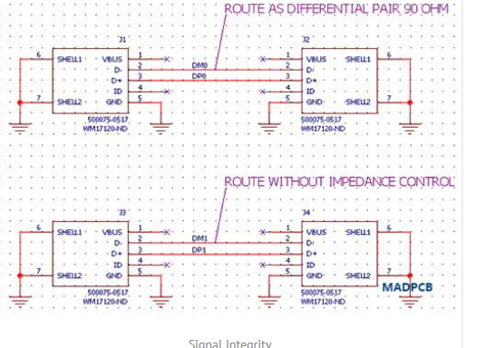
- Differential Pairs: Two closely spaced traces carrying complementary signals
Key Transmission Line Parameters
- Characteristic impedance (Z₀)
- Propagation delay
- Attenuation (loss tangent)
- Crosstalk susceptibility
- Dispersion characteristics
Common Signal Integrity Problems in PCB Transmission Lines
1. Impedance Mismatch and Reflections
Impedance discontinuities occur when the characteristic impedance of the transmission line changes along its path, causing signal reflections. These reflections can lead to:
- Ringing (oscillations at signal transitions)
- Overshoot/undershoot (signal levels exceeding intended voltages)
- Timing jitter (variations in signal timing)
2. Attenuation and Loss Mechanisms
High-frequency signals experience several loss mechanisms:
- Conductor losses: Due to finite conductivity of copper traces
- Dielectric losses: Energy absorbed by the PCB substrate material
- Skin effect: Current crowding at higher frequencies
- Surface roughness: Increased resistance due to uneven copper surfaces
3. Crosstalk
Unwanted coupling between adjacent traces can cause:
- Forward crosstalk (near-end): Coupling in the direction of signal propagation
- Backward crosstalk (far-end): Coupling opposite to the signal direction
4. Power Integrity Issues
Voltage fluctuations in power distribution networks can affect signal quality through:
- Simultaneous switching noise (SSN)
- Ground bounce
- Power supply induced jitter
5. Electromagnetic Interference (EMI)
Poorly designed transmission lines can radiate electromagnetic energy, causing interference with other system components or failing regulatory compliance tests.
Comprehensive Solutions for SI Problems
1. Proper Impedance Control
Impedance Matching Techniques:
- Termination strategies:
- Series termination (source termination)
- Parallel termination (end termination)
- Thevenin termination
- AC termination (capacitive termination)
- Differential termination for high-speed differential pairs
PCB Design Considerations:
- Maintain consistent trace width and height above reference plane
- Use appropriate dielectric materials with stable properties
- Calculate impedance using field solvers or empirical formulas
- Account for manufacturing tolerances (±10% is typical)
2. Minimizing Transmission Line Losses
Conductor Loss Reduction:
- Use wider traces where possible (within impedance constraints)
- Specify smoother copper surfaces (low-profile foils)
- Consider thicker copper weights for critical traces
- Implement embedded planar resistors for termination
Dielectric Loss Mitigation:
- Select low-loss dielectric materials (e.g., Rogers, Isola, or specialized FR-4)
- Use lower dielectric constant (Dk) materials when possible
- Consider hybrid stackups with high-performance materials for critical layers
3. Crosstalk Reduction Techniques
Physical Layout Strategies:
- Maintain adequate spacing between traces (3x dielectric height is a good starting point)
- Route critical traces orthogonally on adjacent layers
- Use guard traces with via stitching for sensitive signals
- Implement ground planes between signal layers
Design Rules:
- Follow the 3W rule (center-to-center spacing ≥ 3x trace width)
- Apply the 20H rule (extend ground plane beyond power plane by 20x dielectric thickness)
- Use differential pairs for high-speed interfaces with proper coupling
4. Advanced Routing Techniques
Length Matching:
- Implement serpentine routing for delay matching
- Use phase tuning features in PCB design software
- Match lengths within timing budgets (typically < 50ps mismatch)
Via Optimization:
- Minimize via stubs (consider backdrilling for thick PCBs)
- Use via-in-pad technology for dense designs
- Implement via shielding for critical signals
- Consider differential via structures for high-speed differential pairs
5. Power Integrity Enhancements
Decoupling Strategies:
- Implement a mix of bulk, ceramic, and high-frequency capacitors
- Place decoupling capacitors close to power pins
- Use plane capacitance (thin dielectrics between power/ground planes)
Power Delivery Network (PDN) Design:
- Use multiple vias for power connections
- Implement split planes carefully with proper bridging
- Perform PDN impedance analysis and optimization
- Consider dedicated power layers in multilayer designs
6. Material Selection and Stackup Design
Key Material Considerations:
- Dielectric constant (Dk) and its stability over frequency
- Dissipation factor (Df) at operating frequencies
- Thermal stability and moisture absorption
- Cost and manufacturability
Stackup Design Guidelines:
- Maintain symmetry to prevent warpage
- Provide adequate reference planes for all signal layers
- Consider mixed dielectric stackups for cost/performance optimization
- Use simulation tools to verify stackup performance
Simulation and Verification Techniques
Pre-layout Simulation
- Perform feasibility studies for critical interfaces
- Model interconnect effects before physical design
- Optimize termination strategies and routing topologies
Post-layout Analysis
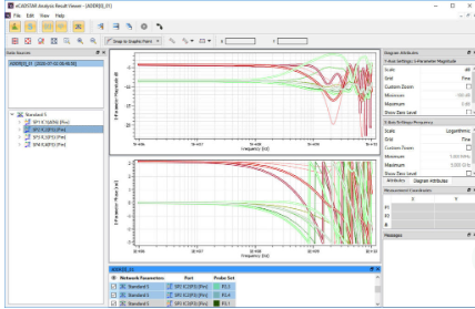
- Extract parasitic parameters (S-parameters, RLGC matrices)
- Perform time-domain reflectometry (TDR) simulations
- Analyze eye diagrams for high-speed serial links
- Verify compliance with relevant standards (PCIe, USB, DDR, etc.)
Measurement and Correlation
- Perform vector network analyzer (VNA) measurements
- Conduct time-domain reflectometry measurements
- Use high-bandwidth oscilloscopes for signal quality verification
- Correlate simulation results with measurements for model refinement
Emerging Technologies and Future Trends
Advanced Materials
- Ultra-low-loss dielectrics for 100+ GHz applications
- Engineered substrates with anisotropic properties
- Embedded passive components for impedance control
Novel Interconnect Technologies
- Photonic interconnects for extremely high bandwidth
- 3D packaging and through-silicon vias (TSVs)
- Co-packaged optics for data center applications
Design Methodologies
- AI-assisted PCB design and optimization
- Automated constraint generation and verification
- Cloud-based collaborative design environments
Conclusion
Solving Signal Integrity problems in PCB transmission lines requires a systematic approach that combines fundamental understanding with practical design techniques. By implementing proper impedance control, minimizing losses, reducing crosstalk, optimizing routing, and ensuring power integrity, designers can create robust PCB layouts that meet increasingly demanding performance requirements.
As signal speeds continue to rise and form factors shrink, the importance of comprehensive SI analysis and design will only grow. Staying current with emerging technologies, materials, and design methodologies will be essential for engineers working on next-generation electronic systems.
The most effective SI solutions come from considering signal integrity throughout the entire design process—from initial architecture through final verification—rather than as an afterthought. By adopting this proactive approach and leveraging available tools and technologies, designers can successfully navigate the challenges of high-speed PCB design and deliver reliable, high-performance products.