How Are the Top and Bottom Layers Connected in a PCB?
Introduction to PCB Layer Connections
Printed Circuit Boards (PCBs) form the foundation of modern electronics, providing both mechanical support and electrical connections between components. As electronic devices have become more complex, PCBs have evolved from simple single-layer designs to sophisticated multi-layer configurations. One of the most fundamental yet crucial aspects of PCB design is understanding how the top and bottom layers connect to create a functional circuit.
In this comprehensive guide, we’ll explore the various methods and technologies used to establish connections between a PCB’s top and bottom layers. We’ll examine through-hole technology, vias, advanced interconnection techniques, design considerations, and troubleshooting approaches. Whether you’re an electronics enthusiast, engineering student, or professional designer, this article will provide valuable insights into this critical aspect of PCB fabrication.
Through-Hole Technology (THT): The Traditional Approach
Understanding Through-Hole Components
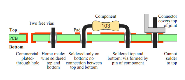
Through-hole technology represents one of the earliest and most straightforward methods for connecting PCB layers. This technique involves drilling holes completely through the PCB substrate and plating the interior surfaces to create conductive pathways. Components with long leads are inserted through these holes and soldered on both sides, creating a secure mechanical and electrical connection between layers.
Through-hole connections offer several advantages:
- Mechanical strength: Components are physically anchored to the board
- Reliability: Robust connections suitable for high-stress environments
- Ease of manual assembly: Simplifies prototyping and repair processes
The Through-Hole Manufacturing Process
The creation of through-hole connections follows a precise sequence:
- Drilling: Holes are drilled through the entire board at designated locations
- Plating: The hole interiors are electroplated with copper to create conductivity
- Component insertion: Leads are threaded through the holes
- Soldering: Solder is applied to both sides (often via wave soldering)
While through-hole technology remains valuable for certain applications, its limitations in high-density designs have led to the development of more advanced interconnection methods.
Vias: The Modern Solution for Layer Interconnection
What Are Vias?
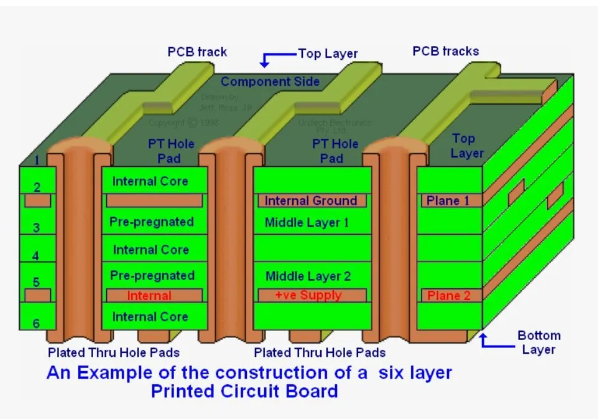
Vias have become the standard method for connecting different layers in modern PCBs. These small, plated holes serve as vertical conduits for electrical signals between layers without accommodating component leads. Via technology enables higher circuit density and more compact designs compared to traditional through-hole approaches.
Types of Vias in PCB Design
- Through-hole vias: Span the entire board thickness, similar to THT but smaller
- Blind vias: Connect an outer layer to one or more inner layers without passing through the entire board
- Buried vias: Connect only inner layers, invisible from the board surface
- Microvias: Extremely small vias (typically <0.15mm) used in high-density designs
The Via Fabrication Process
Modern via creation involves sophisticated techniques:
- Laser drilling: For microvias and high-precision applications
- Photolithography: For defining via locations in complex designs
- Electroless copper deposition: Ensures reliable plating in high-aspect-ratio vias
- Via filling: Conductive or non-conductive materials may fill vias for planarization
Advanced Interconnection Technologies
High-Density Interconnect (HDI) PCBs
As electronic devices shrink, HDI technology has emerged to support more connections in smaller areas:
- Stacked vias: Multiple vias placed directly atop one another
- Staggered vias: Offset vias that conserve space while maintaining connections
- Via-in-pad: Vias placed directly in component pads to save space
Flexible and Rigid-Flex PCB Connections
Specialized applications require innovative approaches:
- Anchoring structures: For reliable layer transitions in flex areas
- Staggered layer transitions: To reduce stress in flexible sections
- Adhesive systems: That maintain conductivity while allowing flexibility
Design Considerations for Reliable Layer Connections
Electrical Factors
Proper layer interconnection requires attention to:
- Current capacity: Via size must match expected current loads
- Signal integrity: Via stub effects on high-speed signals
- Impedance matching: Maintaining consistent impedance through transitions
Thermal Management
Heat affects connection reliability:
- Thermal relief pads: Prevent heat sinking during soldering
- Via spacing: Adequate clearance for heat dissipation
- Thermal vias: Specifically designed for heat transfer
Manufacturing Constraints
Designers must consider:
- Aspect ratios: Hole depth vs. diameter limitations
- Drilling tolerances: Minimum via sizes for different technologies
- Material compatibility: With plating and filling processes
Troubleshooting Common Connection Issues
Open Circuits Between Layers
Diagnosing and resolving failed connections:
- Continuity testing: Identifying open vias or through-holes
- Cross-section analysis: Inspecting plating quality
- Thermal stress testing: Revealing mechanical failure points
Short Circuits and Crosstalk
Addressing unintended connections:
- Insufficient via clearance: Causes adjacent layer shorts
- Plating overhang: Creates bridging risks
- Inadequate shielding: Leads to signal interference
Reliability Challenges
Ensuring long-term connection integrity:
- Thermal cycling effects: On different expansion coefficients
- Mechanical stress: On via structures during operation
- Environmental factors: Such as humidity and corrosion
Future Trends in PCB Layer Interconnection
Emerging Technologies
The frontier of PCB interconnections includes:
- 3D printed electronics: With built-in vertical connections
- Nanoscale vias: For ultra-high density applications
- Optical interconnects: Using light instead of electrons between layers
Materials Innovation
Advanced substrates enabling better connections:
- Low-loss dielectrics: For high-frequency performance
- Thermally stable materials: Reducing interconnection stress
- Self-healing conductors: For improved reliability
Design Automation Tools
Software advancements supporting complex interconnections:
- AI-assisted via placement: Optimizing signal paths automatically
- 3D electromagnetic simulation: Predicting interconnection behavior
- Manufacturability analysis: Flagging potential connection issues early
Conclusion
The methods for connecting PCB top and bottom layers have evolved significantly from simple through-hole connections to sophisticated via technologies enabling modern high-density designs. Understanding these interconnection techniques is fundamental for anyone involved in electronics design, manufacturing, or troubleshooting. As technology progresses, we can expect even more innovative solutions to emerge, pushing the boundaries of what’s possible in PCB layer interconnection while addressing the constant demands for smaller, faster, and more reliable electronic devices.
By mastering the principles outlined in this article—from basic through-hole connections to advanced HDI techniques—designers can create more robust and efficient PCBs. The careful consideration of electrical, thermal, and mechanical factors in layer interconnection remains crucial for successful PCB implementation across all industries and applications.