Identifying and Repairing Signal Integrity Issues in PCB Design
Introduction to Signal Integrity in PCBs
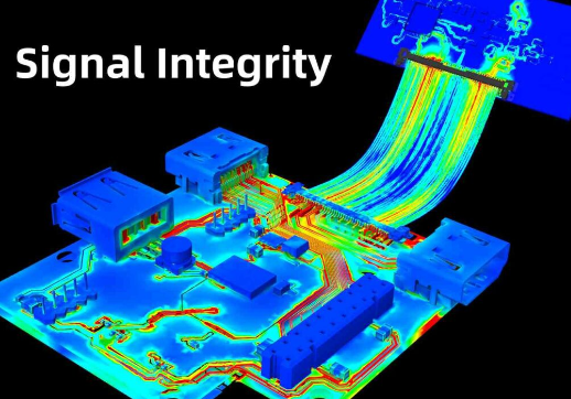
Signal integrity (SI) has become one of the most critical challenges in modern printed circuit board (PCB) design as digital systems continue to operate at higher speeds with lower voltage levels. Signal integrity refers to the quality of electrical signals as they propagate through interconnects on a PCB. When signal integrity is compromised, systems may experience intermittent failures, reduced noise margins, timing violations, or complete functional failure.
As clock frequencies exceed hundreds of MHz and rise times fall into the sub-nanosecond range, PCB traces no longer behave as simple electrical connections but must be treated as transmission lines where impedance control, crosstalk, and electromagnetic interference become significant factors. This article provides a comprehensive guide to identifying common signal integrity problems in PCB designs and practical techniques for repairing these issues.
Common Signal Integrity Problems
1. Impedance Mismatch and Reflections
One of the most fundamental signal integrity issues arises from impedance mismatches along a transmission path. When a signal encounters a change in impedance (typically at connectors, vias, or where trace widths change), a portion of the signal reflects back toward the source. These reflections cause ringing (oscillations at signal edges) and can lead to false triggering of logic gates.
Symptoms:
- Overshoot/undershoot on signal edges
- Ringing after transitions
- Increased rise/fall times
- Timing violations at receivers
2. Crosstalk
Crosstalk occurs when energy from one signal couples to adjacent traces through parasitic capacitance and mutual inductance. There are two types:
- Forward crosstalk (near-end): Appears at the near end of the victim line
- Backward crosstalk (far-end): Appears at the far end of the victim line
Symptoms:
- Unexpected voltage spikes on quiet lines
- Increased jitter on affected signals
- Intermittent logic errors
- Reduced noise margins
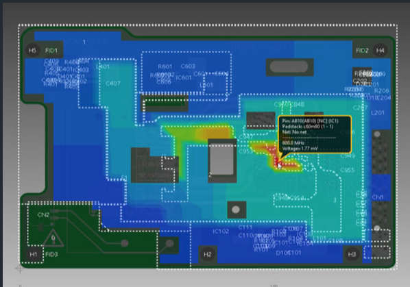
3. Power Integrity Issues
Power distribution network (PDN) problems often manifest as signal integrity issues. When the power supply voltage fluctuates due to inadequate decoupling or high impedance in power planes, signals referencing that power rail are affected.
Symptoms:
- Simultaneous switching noise (SSN)
- Ground bounce
- Increased jitter
- Timing violations correlated with switching activity
4. Electromagnetic Interference (EMI)
Poor signal integrity often leads to excessive electromagnetic radiation from a PCB, which can cause interference with other systems or fail regulatory compliance tests.
Symptoms:
- Radiation emissions exceeding regulatory limits
- Sensitivity to external fields
- Intermittent operation in noisy environments
Identification Techniques
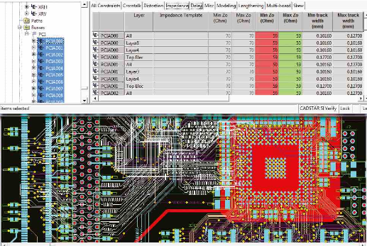
1. Time-Domain Reflectometry (TDR)
TDR is one of the most powerful tools for identifying impedance discontinuities. It works by sending a fast edge down a transmission line and measuring the reflected energy. The time delay and magnitude of reflections indicate the location and severity of impedance mismatches.
2. Eye Diagram Analysis
Eye diagrams provide a wealth of information about signal quality by superimposing many signal transitions. Key parameters measured from eye diagrams include:
- Eye height (voltage margin)
- Eye width (timing margin)
- Jitter (timing uncertainty)
- Rise/fall times
3. Frequency Domain Analysis
Using vector network analyzers (VNAs) or spectrum analyzers can reveal frequency-dependent problems such as:
- Resonances in power distribution networks
- Frequency-specific reflections
- EMI emission peaks
4. Simulation Tools
Modern SI simulation tools can predict problems before manufacturing:
- 2D/3D electromagnetic field solvers
- Transmission line modeling
- IBIS and SPICE simulations
- Power integrity analysis tools
Repair Strategies for Common SI Issues
1. Fixing Impedance Mismatches
Solutions for impedance-related problems:
- Trace geometry adjustment: Modify width and dielectric spacing to achieve target impedance
- Termination resistors: Add series or parallel termination to match impedance
- Via optimization: Use smaller vias, back-drilling, or via stitching for high-speed signals
- Connector selection: Choose connectors with controlled impedance
2. Reducing Crosstalk
Crosstalk mitigation techniques:
- Increased spacing: Follow 3W rule (center-to-center spacing ≥ 3× trace width)
- Ground shielding: Route sensitive signals between ground planes or add guard traces
- Layer stacking: Route adjacent layers orthogonally (horizontal/vertical)
- Differential signaling: Use differential pairs for critical signals
3. Improving Power Integrity
PDN enhancement methods:
- Decoupling capacitors: Proper selection and placement of bypass caps
- Power plane design: Use low-inductance plane pairs with thin dielectrics
- VRM placement: Position voltage regulators close to load points
- Impedance optimization: Target PDN impedance across frequency range
4. EMI Reduction Techniques
EMI control strategies:
- Edge rate control: Use series resistors to slow rise times where possible
- Proper grounding: Maintain low-impedance return paths
- Shielding: Apply copper pours or metal shields over noisy circuits
- Filtering: Add EMI filters to I/O lines
Practical Debugging Workflow
When confronted with signal integrity issues, follow this systematic approach:
- Characterize the problem: Measure and document symptoms (oscilloscope, TDR, etc.)
- Isolate variables: Determine if issue is consistent or intermittent
- Hypothesize root cause: Based on symptoms, identify likely mechanisms
- Implement fixes: Apply targeted corrections (start with least invasive)
- Verify results: Re-measure to confirm improvement
- Iterate: If problem persists, refine hypothesis and try alternative solutions
Case Studies
Case 1: DDR Memory Interface Failures
Symptoms: Random read/write errors at high frequency operation
Analysis: Eye diagram shows collapsed voltage margin and excessive jitter
Root Cause: Impedance discontinuities at via transitions and inadequate power delivery
Solution:
- Redesigned via transitions with smaller drill size and antipads
- Added additional decoupling capacitors near memory chips
- Implemented proper termination scheme
Result: Stable operation at full design speed with sufficient timing margin
Case 2: High-Speed Serial Link Bit Errors
Symptoms: Intermittent CRC errors on PCIe Gen3 link
Analysis: TDR shows impedance variations along route, crosstalk from adjacent clock line
Root Cause: Impedance mismatch at connector interface and insufficient spacing to clock
Solution:
- Added impedance matching network at connector
- Rerouted clock trace with greater separation
- Improved reference plane continuity
Result: Link passed compliance testing with zero bit errors
Prevention Through Design
The most cost-effective approach to signal integrity is designing it in from the beginning:
- Stackup design: Plan layer stack for controlled impedance and good return paths
- Routing rules: Establish and follow constraints for critical signals
- Component placement: Group related circuits and minimize critical path lengths
- Simulation: Verify key interfaces before layout completion
- Design reviews: Have SI experts review before finalizing design
Conclusion
Signal integrity issues in PCBs can be challenging to diagnose and repair, but with systematic analysis and proper tools, most problems can be resolved. The key is understanding the fundamental transmission line principles that govern high-speed digital design and applying appropriate mitigation strategies. By combining careful measurement techniques with targeted corrective actions, designers can achieve robust signal integrity even in complex, high-speed designs.
As data rates continue to increase with new interface standards, signal integrity engineering will remain a critical discipline in electronic product development. Investing in proper design practices, analysis tools, and engineering expertise upfront can prevent costly redesigns and product failures down the line.