Application of laser drilling technology in PCB industry
[Abstract] As the holes on PCB become more and more dense, laser drilling technology becomes more and more important. This paper collects the drilling technology requirements for flexible circuit boards, HDI boards and IC substrates; analyzes three types of laser drilling machines, UV laser drilling, CO2 laser drilling and ultrafast laser drilling, in detail from the three aspects of principle, technical characteristics and usage; at the same time, the application prospects of ultrafast lasers in the PCB industry are prospected.
Introduction
PCB is an important supporting device for the electronic information industry. The development of PCB industry technology needs to adapt to the needs of downstream electronic terminal equipment.
At present, electronic products mainly show two obvious trends: light, thin and short and high speed and high frequency. The application needs of downstream industries have put forward higher requirements for the precision and stability of PCBs.
In recent years, with the continuous development of industries such as smart terminals, smart wearable devices, 5G and cloud computing, the market demand for flexible boards and rigid-flex boards, HDI boards and IC substrates has continued to grow. The number, size and structure of PCB conductor lines and holes will undergo major changes; wires will become smaller, fewer, or even wireless; vias will become smaller, more numerous, or even fully via-hole-free. Therefore, the signal transmission process in the PCB conductor will increasingly take place in the holes [5]. Since the size and surface state of the vias will directly affect the stability and efficiency of signal transmission on the PCB board, how to produce high-quality microvias will become an urgent problem to be solved in PCB manufacturing.
I. Mainstream PCB drilling machines on the market
The most commonly used methods for microvia processing on circuit boards are CNC mechanical drilling and laser drilling.
At present, CNC drilling machines are mainly used to process through holes with a diameter greater than 150μm. When the hole diameter/hole spacing is greater than 150μm/100μm, the efficiency of mechanical drilling will be relatively high. However, mechanical micro-hole processing methods have gradually failed to meet the requirements of micro-hole processing in terms of hole size and position accuracy. The main reasons are: (1) The rigidity of the drill bit with a small diameter is weak and it is very easy to bend during high-speed rotation drilling, resulting in drilling position deviation; (2) The drill bit is extremely fine, has a short life, and is easy to break. When drilling micro-holes below 150μm, the cost is greatly increased [1].
Micro-holes and blind holes with a hole diameter less than 150μm are mostly drilled by laser.
The laser drilling machines in the PCB industry are mainly UV laser drilling machines for drilling soft boards and CO2 laser drilling machines for drilling hard boards, with ultrafast laser drilling machines and composite wavelength laser drilling machines equipped with two wavelength lasers as auxiliary.
2.Technical requirements for laser drilling
2.1 Flexible boards
The diameters of blind holes and through holes in double-sided boards produced by flexible circuit board manufacturers are mainly 100μm and 75μm. There are also 50μm holes produced in mass production, but the production quantity and frequency are very small.
Some manufacturers have begun to verify machines that can drill 30μm micro holes in preparation for the production of higher density FPCs. Existing UV drilling machines can basically meet the drilling needs of the flexible circuit board industry, but with the widespread use of 5G, some composite materials have begun to appear. Traditional UV lasers cannot meet the drilling needs and ultrafast laser drilling machines are needed for drilling.
2.2 HDI boards
HDI boards are a type of circuit board with a relatively high line distribution density using micro blind buried hole technology. The dielectric layer is mixed with a glass fiber yarn layer. It is a type of hard board and accounts for a large proportion of PCBs. The diameter of through holes in the currently mass-produced HDI boards is mainly 75-150μm[2][7].
2.3 IC substrate
IC substrate is a new type of high-end PCB product that has emerged in recent years and is known as the jewel in the crown of PCB. IC substrate is developed on the basis of HDI board. It is a technological innovation that adapts to the rapid development of electronic packaging technology. It has excellent characteristics such as high density, high precision, high performance, miniaturization and thinness.
The aperture of micropores in mass production is mainly 50-100μm, and the minimum aperture in mass production can reach 30μm.
The dielectric layer of IC substrate is divided into two categories: BT and ABF. The BT layer mainly contains glass fiber yarn layer. At present, CO2 laser drilling machine is the main one. There are also some green ultrafast lasers that can drill 40μm micropores. It is reported that on ABF substrate, the minimum aperture of laser drilling can reach 5μm.
3.Principle of laser drilling
The wavelength of laser can range from ultraviolet to infrared (as shown in Figure 1). Currently, UV lasers, visible light lasers, IR lasers, CO2 lasers, etc. are commonly used in industry. Lasers can be divided into: continuous lasers, quasi-continuous lasers, nanosecond lasers, picosecond lasers, femtosecond lasers, etc. according to pulse length. The mechanism and effect of different types of lasers on materials are very different.
At present, the laser drilling machines commonly used in the industry can be divided into two categories according to the light source: UV nanosecond laser drilling machines with a wavelength of 355nm and CO2 laser drilling machines with a wavelength of 9400nm.
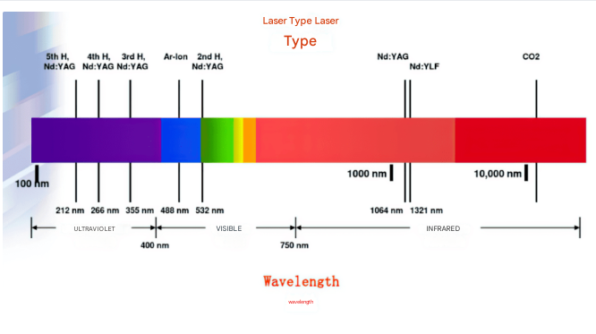
Figure 1 Wavelength distribution of lasers (Source: Huaqiu Electronics)
As shown in Figure 2, the commonly used substrates in PCB boards are copper foil, resin and glass fiber, and the absorption rates of different wavelengths are very different: copper foil has a high absorption rate for UV and a low absorption rate for CO2; the absorption rates of resin and glass fiber for different wavelengths are very different, the absorption rate of resin for UV and CO2 is very high, and the absorption rate of glass fiber for CO2 laser is relatively high.
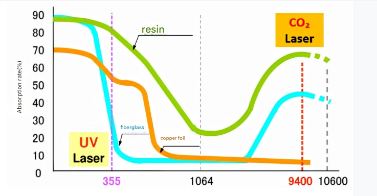
Figure 2 Absorption rate of spectral spectrum of main PCB substrates (Source: Huaqiu Electronics)
Since the substrate has a large difference in absorption of lasers of different wavelengths, the wavelength of laser drilling machine used mainly depends on the material of the dielectric layer: only resin substrates in the dielectric layer use UV laser drilling machines, and glass fiber substrates in the dielectric layer use CO2 laser drilling machines.
3.1 UV nanosecond laser drilling
Figure 3 Drilling effect of JPT UV laser drilling machine
The mechanism of UV laser drilling is mainly photochemical ablation: the photons of short-wavelength lasers have very high energy (more than 2eV). High-energy photons can destroy the long molecular chains of organic materials, turning them into particles and detaching them from the processed materials. Under the action of continuous external UV laser, the substrate material continuously escapes to form micropores.
Main features of UV laser drilling:
Photochemical ablation is the main method, with little thermal ablation reaction and little carbide produced, and the cleaning before hole formation is very simple;
It can directly remove copper and can be drilled directly, without pre-treatment of copper before drilling;
At present, the minimum size of holes that can be drilled by several commonly used UV laser drilling machines is 25μm.
3.2 CO2 optical drilling
If the dielectric layer material has glass fiber, a CO2 drilling machine is generally used. The principle of CO2 laser drilling is mainly photothermal ablation: the processed material continuously absorbs high-energy laser, is heated to melt in a very short time, and then the temperature continues to rise to vaporize the material, and finally evaporates to form micropores.
In actual production, the process method of direct ablation of ultra-thin copper foil is generally adopted. The steps are as follows:
The copper foil thickness is reduced from 12μm to about 9μm by etching;
The copper foil is browned or blackened to make the copper surface rough and dark, which is conducive to energy absorption;
The copper layer is first removed by laser, and then the dielectric layer is removed to achieve drilling.
The CO2 laser drilling speed is much faster than UV laser drilling. However, processing is required before and after drilling.
Due to the existence of diffraction limit, CO2 laser can only be focused to a minimum of about 35μm through an optical lens [3]. In actual mass production, holes with an aperture of 75-150μm are generally drilled.
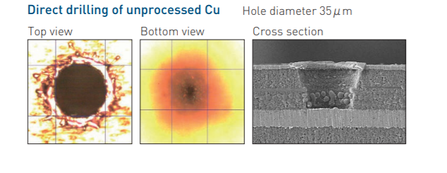
Figure 4 CO2 laser drilling machine drilling 35μm hole
(Source: Via Mechanics official website)
3.3 Ultrafast laser drilling
With the increasing application of ultrafast lasers in industry and the increasing requirements of the PCB industry for hole diameter and hole shape, some equipment manufacturers have begun to try to use ultrafast lasers to drill holes in PCB substrates.
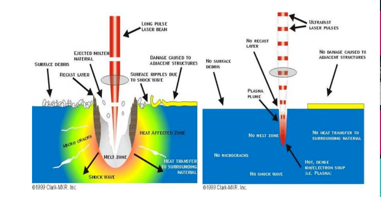
Figure 5 Comparison of nanosecond and ultrafast laser and material action mechanisms
Ultrafast lasers have the characteristics of ultrahigh peak power, ultrashort pulse width and short action time. During processing, the heat diffusion distance inside the material is short, and it has non-thermal melting processing characteristics, which has unique advantages in micro-nano processing [4]. Ultrafast laser processing eliminates defects such as “thermal damage” and “thermal internal stress”, and has three obvious advantages for PCB drilling:
It can be applied to almost all materials in the manufacturing industry for processing;
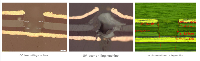
Figure 6 Effects of different laser drilling machines on processing PTFE materials
As shown in Figure 7, UV nanosecond laser drilling machines are completely unable to drill materials with PTFE as the dielectric layer, while UV picosecond drilling can control the shrinkage of the glue within 10μm.
The quality of drilling is close to perfect. As shown in Figure 7, ultrafast laser drilling solves the problems of melting into balls, craters, residual glue at the bottom of the hole, and protruding glass fibers after long pulse laser processing;
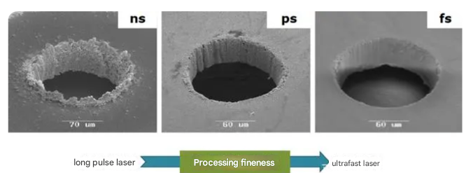
Figure 7 Drilling effects of lasers with different pulse widths (Source: Songshan Lake Materials Laboratory)
The processed vias have very low wall roughness (≤0.1μm), which can significantly reduce signal transmission loss and distortion in high-frequency signal transmission, especially in the packaging substrate assembly of stacked hole structures. It has excellent signal transmission performance [6].
Conclusion
In summary, in current PCB manufacturing, through holes larger than 150μm are mainly drilled mechanically; 50-150μm vias containing glass fiber are mainly drilled by CO2 laser drilling machines, and materials without glass fiber are mainly drilled by UV laser drilling machines. UV and CO2 drilling machines are capable of drilling most PCB vias at this stage.
However, as the size of PCBs develops towards miniaturization and signal transmission develops towards high frequency, the apertures that need to be drilled are getting smaller and smaller, the quality requirements of the holes are getting higher and higher, and the materials of the dielectric layer are constantly increasing. The traditional laser drilling method will gradually fail to meet the drilling needs, just like the CNC mechanical drilling machine.
Ultrafast laser drilling will not have the phenomenon of heat diffusion and heat conduction to the surrounding area. The processed via hole wall does not have problems such as melting into balls, craters, residual glue at the bottom of the hole, and protruding glass fibers. Almost all thinner materials can be removed. This laser drilling method with near-perfect drilling quality will be widely used in PCB manufacturing.