PCB Red Dye Penetration Test: Definition, Process, and Applications
1. Introduction
Printed Circuit Boards (PCBs) are essential components in modern electronic devices, ensuring proper electrical connections between components. However, defects such as micro-cracks, poor solder joints, or hidden fractures can lead to intermittent failures or complete malfunctions. To detect these flaws, the Red Dye Penetration Test (Red Dye Test or Red Ink Test) is widely used in PCB manufacturing and failure analysis.
This article explores the definition, methodology, applications, advantages, and limitations of the PCB Red Dye Penetration Test, providing a comprehensive understanding of its role in quality assurance.
2. Definition of PCB Red Dye Penetration Test
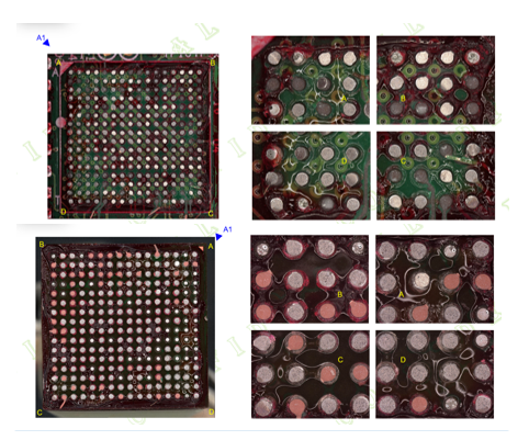
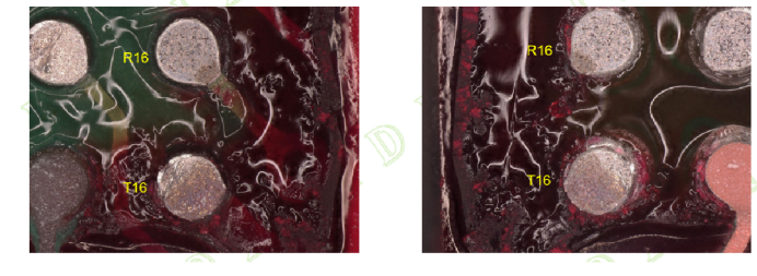
The Red Dye Penetration Test is a destructive testing method used to identify micro-cracks, voids, and other hidden defects in solder joints, plated through-holes (PTHs), and PCB substrates. The test involves applying a red-colored dye penetrant (typically a fluorescent or high-visibility dye) onto the PCB assembly. The dye seeps into any existing cracks or openings due to capillary action. After cleaning the excess dye, the PCB is inspected under magnification to reveal the extent of penetration, pinpointing failure points.
This test is particularly useful for diagnosing intermittent electrical failures where visual inspection alone cannot detect the root cause.
3. Process of Red Dye Penetration Testing
The Red Dye Test follows a systematic procedure to ensure accurate defect detection:
Step 1: Sample Preparation
- The PCB assembly is cleaned to remove contaminants (flux residues, oils, dust) that may interfere with dye penetration.
- If the test targets a specific failure (e.g., an intermittent connection), the area of interest is identified.
Step 2: Dye Application
- A low-viscosity red dye (often epoxy-based) is applied to the target area using a brush, spray, or immersion method.
- The dye must fully cover the suspected defect zones (e.g., solder joints, vias, or component leads).
Step 3: Dye Penetration
- The PCB is placed in a controlled environment (sometimes under slight vacuum or pressure) to enhance dye penetration into micro-cracks.
- The dye is allowed to seep for a specified time (typically 10–30 minutes).
Step 4: Excess Dye Removal
- The PCB is rinsed with a solvent (e.g., isopropyl alcohol) to remove surface dye while retaining the dye trapped in defects.
- Care must be taken to avoid excessive cleaning, which could wash out the dye from cracks.
Step 5: Inspection & Analysis
- The PCB is dried and carefully dissected (if necessary) to expose internal layers.
- Under magnification (microscope or optical inspection system), the red dye traces highlight defect locations.
- The extent of dye penetration helps determine the severity of the defect.
Step 6: Documentation & Reporting
- Findings are documented with images and descriptions of defect locations.
- The results guide corrective actions in manufacturing or design improvements.
4. Applications of Red Dye Testing in PCB Analysis
The Red Dye Penetration Test is widely used in:
A. Solder Joint Failure Analysis
- Detects hairline cracks in BGA (Ball Grid Array), QFN (Quad Flat No-leads), and other solder joints.
- Identifies cold solder joints, insufficient wetting, or voids in reflow/wave soldering.
B. Plated Through-Hole (PTH) Inspection
- Reveals cracks in barrel plating or poor via connections.
- Helps diagnose intermittent open circuits in multilayer PCBs.
C. PCB Laminate & Substrate Defects
- Detects delamination, micro-fractures, or resin cracks in the base material.
D. Reliability Testing
- Used in thermal cycling and vibration stress tests to assess long-term durability.
E. Root Cause Analysis in Field Failures
- Helps determine why a PCB failed in real-world conditions.
5. Advantages of Red Dye Testing
- High Sensitivity: Detects micron-level cracks invisible to X-ray or visual inspection.
- Cost-Effective: Less expensive than advanced techniques like CT scanning.
- Simple Methodology: No complex equipment required—basic tools suffice.
- Versatile: Applicable to various PCB types (rigid, flex, HDI).
6. Limitations & Challenges
- Destructive Nature: The PCB is often destroyed during inspection.
- Limited to Surface-Connected Defects: Cannot detect internal voids unless cross-sectioned.
- Subjectivity in Interpretation: Requires skilled technicians for accurate analysis.
7. Comparison with Other PCB Testing Methods
| Test Method | Detection Capability | Destructive? | Cost |
|---|---|---|---|
| Red Dye Test | Micro-cracks, voids | Yes | Low |
| X-ray Inspection | Internal voids, BGA defects | No | High |
| Microsectioning | Cross-sectional defects | Yes | Medium |
| AOI (Automated Optical Inspection) | Surface defects | No | Medium |
8. Conclusion
The PCB Red Dye Penetration Test remains a vital tool for failure analysis, especially in detecting hidden solder joint and via defects. While it has limitations, its simplicity, effectiveness, and low cost make it indispensable in PCB quality control.
By integrating the Red Dye Test with other inspection methods (e.g., X-ray or microsectioning), manufacturers can ensure higher reliability and performance of electronic assemblies.