How to Thicken Power Traces in PCB Design: A Comprehensive Guide
Introduction
Printed Circuit Board (PCB) design requires careful consideration of power distribution networks, with power trace sizing being one of the most critical aspects. Properly sized power traces ensure reliable operation, prevent overheating, and maintain voltage stability across the board. This 2000-word guide explores the techniques, calculations, and best practices for thickening power traces in PCB designs.
Understanding Current Carrying Capacity
The Fundamentals of Trace Current Capacity
The current carrying capacity of a PCB trace depends on several factors:
- Cross-sectional area: Primarily determined by trace width and copper thickness
- Temperature rise: The acceptable temperature increase above ambient
- Copper thickness: Typically specified in ounces (oz), where 1 oz equals 1.37 mils (34.79 μm)
- Ambient conditions: Including airflow and surrounding components
IPC-2152 Standard
The IPC-2152 standard provides the most current guidelines for determining appropriate trace widths based on:
- Current requirements
- Allowable temperature rise
- Copper weight
- Board material
- Presence of internal vs. external layers
Calculating Required Trace Width
Basic Calculation Methods
- Using IPC-2152 Nomographs:
- Graphical tools that relate current, temperature rise, and trace width
- Available in the IPC standard documentation
- Online Calculators:
- Numerous web-based tools implement IPC-2152 calculations
- Example: Saturn PCB Toolkit
- Empirical Formulas:
Width [mils] = (Current [A] / (k * (Temp Rise [°C])^b))^(1/c)Where k, b, and c are constants based on copper weight and layer position
Practical Example Calculation
For a 2A current with 10°C temperature rise on external 1 oz copper:
- Using IPC-2152: Approximately 30 mil width
- Using old IPC-2221: Would sugg
- est about 60 mil (demonstrating how standards have evolved)

Techniques for Thickening Power Traces
Basic Trace Widening Methods
- Manual Routing with Increased Width:
- Set power trace width in design rules before routing
- Most EDA tools allow net-specific width rules
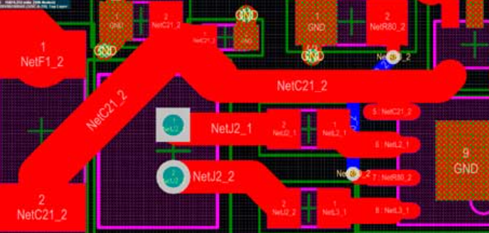
- Using Copper Pours (Polygons):
- Create filled areas connected to power nets
- Particularly effective for power planes or distribution areas
- Tapered Transitions:
- Gradually widen traces from IC pins to main distribution
- Prevents sudden impedance changes
Advanced Methods
- Multi-Layer Distribution:
- Use multiple layers with vias to parallel current paths
- Reduces effective resistance and inductance
- Embedded Bus Bars:
- For very high current applications
- Thick metal bars incorporated into the PCB stackup
- External Bus Bars:
- Supplemental conductors attached to the PCB surface
Design Tool Implementation
Setting Up Design Rules
In most PCB EDA software (Altium, KiCad, Eagle):
- Net Class Rules:
- Create a “Power” net class
- Assign appropriate width constraints
- Differential Width Rules:
- Set minimum, preferred, and maximum widths
- Allow for neck-downs when necessary
- Layer-Specific Rules:
- Account for different current capacities on inner vs. outer layers
Practical EDA Tips
- Altium Designer:
- Use “Polygon Pours” with net associations
- Implement “xSignals” for power distribution analysis
- KiCad:
- Create “Track Width” constraints in the Board Setup
- Use “Zone” tools for copper pours
- Cadence Allegro:
- Utilize “Constraint Manager” for power nets
- Implement “Shape” objects for custom copper areas
Thermal Considerations
Heat Dissipation Techniques
- Thermal Relief Pads:
- Prevent heat sinking to large planes during soldering
- While maintaining good electrical connection
- Copper Balancing:
- Distribute thermal mass evenly
- Prevent localized hot spots
- Via Stitching:
- Multiple vias to transfer heat between layers
- Also improves current carrying capacity
Calculating Temperature Rise
Use the modified Joule heating equation for PCB traces:
ΔT = (I² * R * θ) / (ρ * A * L)Where:
- ΔT = Temperature rise
- I = Current
- R = Resistance
- θ = Thermal resistance
- ρ = Resistivity of copper
- A = Cross-sectional area
- L = Length
Manufacturing Considerations
Copper Weight Selection
Common options:
- 1 oz (35 μm): Standard for most consumer electronics
- 2 oz (70 μm): For higher current applications
- 3 oz (105 μm): Specialized high-current designs
- 4+ oz (140+ μm): Extreme current requirements
Fabrication Limitations
- Minimum Spacing:
- Thicker copper requires wider spacing
- Typical rule: spacing ≥ copper thickness
- Etching Challenges:
- Thicker copper needs wider minimum traces
- Tighter tolerances on finished widths
- Cost Implications:
- Heavier copper weights increase board cost
- May require specialized processes

High-Current Design Strategies
When Standard Traces Aren’t Enough
- Solder Mask Defined (SMD) Traces:
- Apply solder over traces to increase cross-section
- Requires assembly process coordination
- Solder Wire Supplementation:
- Hand-soldering additional wire along traces
- Common in hobbyist and prototype scenarios
- Copper Coin Integration:
- Embedded thick copper pieces in the PCB
- For localized high-current requirements
Parallel Path Techniques
- Multiple Traces in Parallel:
- Several thinner traces instead of one thick one
- Helps with routing congestion
- Multi-Layer Distribution:
- Route power on multiple layers
- Connect with numerous vias
Verification and Testing
Design Rule Checks (DRC)
Ensure your EDA software checks for:
- Minimum width violations
- Current density limits
- Thermal relief compliance
Simulation Methods
- DC Analysis:
- Verify voltage drop meets requirements
- Identify high-resistance segments
- Thermal Simulation:
- Predict temperature distribution
- Validate cooling strategies
- Current Density Analysis:
- Highlight potential electromigration issues
- Identify current crowding areas
Common Pitfalls and Solutions
Frequent Design Mistakes
- Inadequate Neck-Down Handling:
- Solution: Implement smooth transitions
- Via Current Limitations:
- Solution: Use multiple vias in parallel
- Ignoring Layer Differences:
- Solution: Set layer-specific rules
- Overlooking Return Paths:
- Solution: Design complete current loops

Future Trends in Power Distribution
Emerging Technologies
- 3D-Printed Conductors:
- Additive manufacturing of thick traces
- Integrated Cooling Channels:
- PCB-embedded liquid cooling
- Superconducting Materials:
- For extreme current density applications
- AIPCB (Additive-Integrated PCB):
- Combining printed and traditional PCB tech
Conclusion
Proper power trace sizing is fundamental to reliable PCB design. By understanding current requirements, applying appropriate calculation methods, and implementing robust design techniques, engineers can ensure stable power distribution across their circuits. Modern EDA tools provide powerful features for managing power traces, but designers must still apply sound engineering judgment. As power requirements continue to increase while board space decreases, innovative approaches to power distribution will become increasingly important in PCB design.
Remember that while thicker traces solve many power distribution problems, they also introduce new challenges in routing density, manufacturing, and cost. The optimal design always balances electrical requirements with practical constraints, making power trace design both a science and an art.
