Simplifying the Migration from PCB to PLD: Strategies and Best Practices
Introduction
The electronics design landscape has undergone significant transformation in recent decades, with Programmable Logic Devices (PLDs) increasingly replacing traditional printed circuit board (PCB) implementations for many applications. This migration offers numerous advantages, including reduced time-to-market, lower production costs for medium-volume runs, and unparalleled design flexibility. However, the transition from PCB-based designs to PLD solutions presents several technical challenges that can hinder adoption if not properly addressed.
This article explores comprehensive strategies to simplify the migration process from PCB to PLD implementations. We’ll examine the fundamental differences between these approaches, analyze common migration challenges, and present practical solutions to streamline the transition. By following these guidelines, engineering teams can leverage the benefits of programmable logic while minimizing redesign efforts and maintaining system reliability.
Understanding the Fundamental Differences
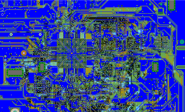
Before attempting migration, it’s crucial to understand the architectural distinctions between PCB and PLD implementations:
- Physical vs. Logical Implementation: PCBs represent designs through physical components and copper traces, while PLDs implement functionality through configurable logic blocks and programmable interconnects.
- Discrete vs. Integrated Timing: PCB designs typically have discrete timing characteristics for each component, whereas PLDs require careful synchronous design practices with centralized clock management.
- Fixed vs. Reconfigurable Functionality: PCBs offer fixed functionality once manufactured, while PLDs can be reprogrammed even after deployment.
- Parallel vs. Resource-Constrained Operation: PCB designs can theoretically implement unlimited parallel operations (given sufficient board space), while PLDs operate within finite logic resource constraints.
These fundamental differences necessitate a thoughtful migration approach rather than a direct one-to-one translation of PCB functionality to PLD implementation.
Pre-Migration Assessment
1. Application Suitability Analysis
Not all PCB designs are ideal candidates for PLD migration. Conduct a thorough evaluation considering:
- Performance Requirements: Assess whether the target PLD can meet timing constraints, especially for high-speed interfaces.
- I/O Characteristics: Verify that the PLD package can accommodate all necessary I/Os with appropriate voltage levels.
- Power Consumption: Compare the power requirements of the existing PCB solution with projected PLD consumption.
- Cost Considerations: Evaluate the economic viability based on production volume and lifecycle expectations.
2. Functional Decomposition
Break down the PCB design into functional blocks to identify:
- Digital vs. analog components (PLDs primarily handle digital functions)
- Clock domains and timing requirements
- Data flow and critical paths
- Interface requirements (memory, peripherals, communication protocols)
3. Resource Estimation
Perform preliminary resource estimation for:
- Logic elements (LUTs, registers)
- Memory blocks
- DSP slices
- Clock management tiles
- I/O banks
Tools like the target PLD vendor’s resource estimator can help determine if the design will fit within the selected device.
Migration Methodology
1. Interface Preservation Strategy
Maintaining compatibility with existing system interfaces is crucial for successful migration:
a) Pinout Compatibility:
- Map PCB connections to PLD pins while considering bank constraints and voltage levels
- Use I/O buffers to match electrical characteristics when necessary
- Implement any required level shifting within the PLD if possible
b) Protocol Preservation:
- Replicate communication protocols exactly when interfacing with existing components
- Consider protocol IP cores available from the PLD vendor
- Implement timing-accurate state machines for custom protocols
c) Signal Integrity Considerations:
- Analyze PLD drive strength requirements compared to original PCB implementation
- Implement proper termination strategies
- Consider using PLD features like programmable slew rate control
2. Timing Domain Transformation
PCB designs often employ multiple clock domains with informal synchronization. PLD implementations require more rigorous clock management:
a) Clock Domain Analysis:
- Identify all clock sources in the original design
- Document clock frequencies and phase relationships
- Note any derived clocks (dividers, PLL outputs)
b) Synchronization Strategy:
- Implement proper clock domain crossing techniques
- Use FIFOs or handshake protocols for inter-domain communication
- Leverage PLD clock management resources (PLLs, MMCMs)
c) Timing Constraints:
- Develop comprehensive timing constraints for the PLD implementation
- Include clock definitions, input/output delays, and false paths
- Validate constraints through static timing analysis
3. Analog Functionality Handling
PLDs primarily handle digital logic, requiring special consideration for analog portions:
a) Identify Analog Components:
- Separate analog functions (filters, sensors, RF) from digital logic
- Determine which analog components must remain discrete
- Consider integrated analog options (ADCs in some PLDs)
b) Digital Replacement Options:
- Implement digital filters instead of analog equivalents when possible
- Use PWM with external filtering for simple DAC functionality
- Consider external analog front-ends for critical analog processing
c) Mixed-Signal Integration:
- Evaluate system partitioning between PLD and remaining analog components
- Optimize board layout for mixed-signal performance
- Implement proper grounding and power distribution

Implementation Techniques
1. Hierarchical Design Approach
Adopt a structured design methodology that mirrors the PCB’s functional organization:
a) Module-Level Correspondence:
- Create PLD modules that correspond to PCB functional blocks
- Maintain similar interfaces between modules
- Document module interactions as per the original design
b) Verification Strategy:
- Develop testbenches for each module based on PCB specifications
- Reuse PCB test vectors when available
- Implement hardware-in-the-loop testing for critical functions
2. Resource Optimization
PLD resources differ fundamentally from PCB components, requiring optimization:
a) Logic Utilization:
- Implement state machine optimizations
- Use resource sharing where appropriate
- Consider time-multiplexing for non-critical paths
b) Memory Management:
- Map PCB memory components to PLD block RAM
- Implement memory controllers for external memories
- Optimize memory access patterns
c) DSP Implementation:
- Replace discrete arithmetic components with PLD DSP slices
- Pipeline arithmetic operations for better performance
- Consider using vendor-supplied DSP IP cores
3. Verification and Validation
Ensure functional equivalence between PCB and PLD implementations:
a) Functional Simulation:
- Develop comprehensive testbenches covering all operational modes
- Verify timing-critical paths through post-place-and-route simulation
- Compare simulation results with PCB measurements
b) Hardware Verification:
- Create verification test suites that exercise all interfaces
- Implement built-in self-test (BIST) functionality where possible
- Perform side-by-side comparison with original PCB when feasible
c) Performance Validation:
- Measure timing characteristics against original specifications
- Validate power consumption under various operating conditions
- Test under extreme operating conditions (temperature, voltage)
Tools and Automation
Leverage available tools to streamline the migration process:
1. Migration-Specific Software
- Use schematic capture tools that support both PCB and PLD design
- Implement scripting for automated netlist translation
- Develop custom scripts for design rule checks specific to migration
2. Vendor-Specific Resources
- Utilize migration guides and application notes from PLD vendors
- Take advantage of IP cores that match common PCB functions
- Participate in vendor migration workshops or training
3. Design Automation
- Create parameterized modules for frequently used functions
- Develop template designs for common migration scenarios
- Implement automated verification testbenches
Common Pitfalls and Mitigation Strategies
Be aware of these frequent migration challenges:
- Unrealistic Resource Expectations:
- Mitigation: Perform detailed resource estimation early
- Solution: Consider larger PLD or optimize design
- Timing Closure Difficulties:
- Mitigation: Implement proper synchronous design practices
- Solution: Add pipeline stages for critical paths
- I/O Limitations:
- Mitigation: Complete thorough pinout analysis
- Solution: Use external buffers or multiplexing
- Power Management Issues:
- Mitigation: Perform power estimation early
- Solution: Implement power-aware design techniques
- Verification Gaps:
- Mitigation: Develop comprehensive test plans
- Solution: Implement hardware co-verification
Post-Migration Considerations
After successful migration, address these important aspects:
- Field Updates and Maintenance:
- Implement PLD configuration management
- Develop field update capability
- Document version control procedures
- Lifecycle Management:
- Monitor PLD obsolescence
- Plan for future migrations
- Document design for possible future transfers
- Performance Optimization:
- Identify areas for further resource optimization
- Consider speed-grade improvements
- Evaluate power reduction opportunities
Conclusion
Migrating from PCB to PLD implementations offers significant advantages but requires careful planning and execution. By following the structured approach outlined in this article—beginning with thorough assessment, proceeding through methodical implementation, and concluding with comprehensive verification—engineering teams can successfully transition designs while minimizing risk and maximizing the benefits of programmable logic.
Key takeaways for successful migration include:
- Understanding the fundamental differences between PCB and PLD paradigms
- Performing detailed pre-migration analysis
- Maintaining interface compatibility
- Implementing rigorous timing management
- Leveraging available tools and automation
- Avoiding common pitfalls through proactive planning
As PLD technologies continue to advance, with increasing capabilities and decreasing costs, the economic and technical case for migration grows stronger. By adopting these best practices, organizations can streamline their migration processes and more readily capitalize on the flexibility, integration, and time-to-market advantages that PLD solutions offer.
The future of electronic design will likely see even greater convergence between traditional PCB and programmable logic approaches, with advanced tools further simplifying the transition between implementation methods. By mastering migration techniques today, design teams position themselves to take full advantage of these evolving technologies tomorrow.

