PCB Outline Processing Method Overview: Technology and Application Detailed Explanation
Introduction
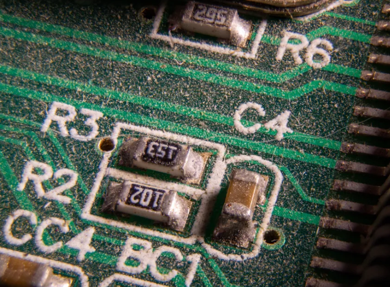
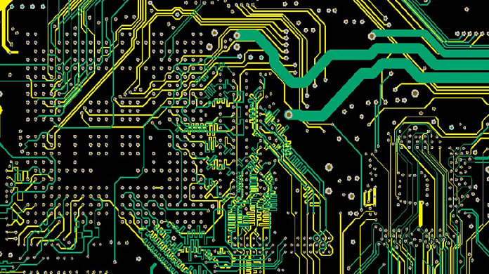
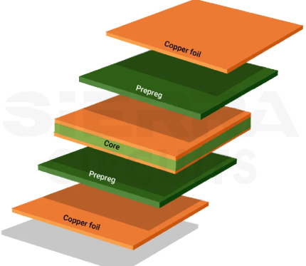
Printed Circuit Boards (PCBs) serve as the fundamental building blocks of modern electronics, providing mechanical support and electrical connections for electronic components. While much attention is often given to the intricate conductive pathways etched onto PCB substrates, the physical shaping and finishing of these boards are equally critical to their functionality and reliability. PCB Outline Processing (Outline Processing) encompasses all processes involved in shaping the board’s physical dimensions, creating cutouts, slots, and edge finishes that enable proper fitment within electronic devices.
The importance of precise Outline Processing cannot be overstated in contemporary electronics manufacturing. As devices continue to shrink in size while increasing in complexity, PCB outlines must adhere to increasingly stringent tolerances—often within ±0.1mm or better. Furthermore, the chosen processing method directly affects production costs, production cycles, and final product quality. From simple mechanical milling to advanced laser cutting, manufacturers must select the most appropriate processing technology based on material properties, design complexity, and production volume requirements.
This comprehensive article will systematically examine all major PCB outline processing methods, analyzing their technical principles, applicable scenarios, and relative advantages and disadvantages. We divide these technologies into three categories: traditional mechanical processing methods, advanced non-contact processing methods, and special processing technologies. By gaining a deeper understanding of these processing options, design engineers and manufacturing professionals can make more informed decisions and optimize their PCB production processes.
Traditional Mechanical Processing Methods
1. CNC Milling
CNC Milling remains the most widely used PCB outline processing technology, especially for small and medium-volume production and high-complexity designs. The process uses a computer-controlled rotating cutting tool to accurately remove substrate material through a multi-axis motion system.
Process Characteristics:
- Use carbide milling cutters with diameters of 0.8-3.175mm
- Typical cutting speeds: 60,000-120,000 RPM
- Achieve positioning accuracy of ±0.05mm
- Support straight and curved cutting paths
Advantages:
- High flexibility: Can process contours, slots and internal cuts at the same time
- Excellent quality: Smooth edges and minimal burrs (maintained by appropriate tools)
- Economical: Suitable for small and medium batch production (100-10,000 pieces)
- Material compatibility: Can process a variety of materials such as FR-4, metal substrates, flexible circuits, etc.
Limitations:
- Mechanical stress may cause deformation of thin plates (0.4mm)
- Tool wear affects long-term processing consistency
- Complex contour processing time is long
Application scenarios: Prototype development, multi-variety small batch production, PCBs with complex internal features
2. Punching
Punching is an efficient solution for high-volume PCB production, especially for standardized designs. The process uses custom molds to achieve instant molding through mechanical pressure.
Technical Parameters:
- Typical pressure: 20-100 tons
- Production speed: up to 1,200 times/hour
- Mold life: about 100,000 times (depending on the material)
- Minimum hole diameter: 1.2 times the board thickness
Key Benefits:
- Unparalleled production efficiency: extremely low unit cost
- Excellent consistency: suitable for tight tolerance requirements
- Edge quality: no burr formation
Challenges:
- High initial tooling cost ($3,000-15,000)
- Poor flexibility for design changes
- Not suitable for thick board (>3.2mm) processing
Best Practices: Standardized designs with annual production exceeding 50,000 pieces, especially consumer electronics PCBs.
3. Shearing
Shearing is the simplest and most economical contour processing method for rectangular PCBs, suitable for low-complexity, high-volume production.
Operation specifications:
- Maximum processing thickness: usually 3-5mm
- Length accuracy: ±0.2mm
- Straightness: 0.1mm/300mm
Advantage areas:
- Extremely low processing costs
- Processing of oversized PCBs (up to 1.2m×2.4m)
- Simple equipment maintenance
Quality considerations:
- Tiny cracks may appear on the edges
- Straight-line cutting only
- Board corners require subsequent processing
Typical applications: Simple designs such as low-cost power boards and LED lighting boards.
Advanced non-contact processing methods
1. Laser Cutting
Laser cutting technology achieves precise material removal through the ablation of high-energy laser beams, and has become an important choice for precision PCB contour processing.
Technical parameters:
- Common laser types: CO₂ (9.4μm) and UV (355nm)
- Cutting thickness: 0.05-3mm
- Positioning accuracy: ±0.01mm
- Minimum slit width: 0.05mm
Process advantages:
- No mechanical stress: Suitable for ultra-thin plates (0.1mm) and brittle materials
- Complex geometry capability: Can process any curve
- High degree of automation: Directly driven by CAD files
Material considerations:
- FR-4 materials require multiple cuts
- Polyimide performs well
- Metal substrates require higher power
Operational cost analysis: Although the equipment investment is high ($100,000-500,000), the tool has zero loss and is suitable for production environments with frequent line changes.
2. Water Jet Cutting
Water jet cutting uses high-pressure water (sometimes mixed with abrasives) to erode materials, and is suitable for processing special PCB materials.
Performance indicators:
- Pressure range: 300-600MPa
- Cutting speed: 50-500mm/min
- Thickness capacity: up to 25mm
- Surface roughness: Ra 3.2-12.5μm
Unique value:
- Cold processing characteristics: no heat-affected zone
- Material versatility: can cut ceramics and metal composites
- Environmental protection: no harmful gases are generated
Application restrictions:
- Slightly rough edge quality
- Large equipment noise (above 85dB)
- High operating cost (abrasive consumption)
Typical use: Processing of thick copper plates and mixed material substrates for high-power electronics.
Special Processing Technology
1. Plasma Cutting
Plasma cutting is mainly used for efficient processing of metal-based PCBs (such as aluminum substrates).
Process Features:
- Cutting speed can reach 10m/min
- Thickness range: 0.5-50mm
- Cutting width: 1-2mm
Quality Control Points:
- Heat-affected zone control
- Slag removal
- Surface oxidation protection
Industry Applications: High-power LED heat dissipation substrates, power electronic modules.
2. Chemical Milling
Chemical milling achieves material removal through controlled chemical etching and is suitable for the processing of ultra-thin flexible circuits.
Key technical parameters:
- Etching rate: 20-50μm/min
- Side etch control: 0.5-1:1 (line width: etching depth)
- Minimum feature size: 0.075mm
Process advantages:
- Stress-free processing
- Can process multiple layers of panels at the same time
- Microstructure processing capabilities
Environmental considerations: A professional waste liquid treatment system is required, suitable for production facilities with strict environmental protection qualifications.
Processing Method Selection Guide
Decision Matrix Analysis
| Considerations | CNC Milling | Stamping | Laser | Water Jet | Chemical Milling |
|---|---|---|---|---|---|
| Initial Cost | $$ | $$$$ | $$$ | $$$ | $$ |
| Unit Cost | $$ | $ | $$$ | $$ | $$ |
| Processing Accuracy | 0.05mm | 0.1mm | 0.01mm | 0.1mm | 0.025mm |
| Material Adaptability | High | Medium | Medium | Very High | Limited |
| Design Flexibility | Very High | Low | High | High | Medium |
| Production Speed | Medium | Very High | Medium-High | Low-Medium | Medium |
Industry Application Trends
- Consumer electronics: Laser cutting is becoming increasingly popular, meeting the needs of ultra-thin and special-shaped designs
- Automotive electronics: CNC milling still dominates due to its reliability and material compatibility
- Aerospace: Water jet cutting is increasingly used in composite substrate processing
- Medical equipment: UV laser processing has become the first choice for PCBs of micro-implant devices
Quality inspection standards
Key inspection indicators
- Dimension tolerance: Classified according to IPC-6012 standard
- Class 1: ±0.15mm
- Class 2: ±0.10mm
- Class 3: ±0.05mm
- Edge quality:
- Burr height: ≤25μm (microscope inspection)
- Delamination defect: According to IPC-TM-650 2.4.22
- Carbonization evaluation: a unique indicator for laser processing
- Mechanical strength:
- Bending test: JIS C 5016 standard
- Peel strength: IPC-TM-650 2.4.8
Process control methods
- Statistical process control (SPC): CPK of key dimensions ≥ 1.33
- Automatic optical inspection (AOI): 100% contour scanning
- Destructive testing: Sampling each batch for micro-section analysis
Future technology outlook
Emerging processing technologies
- Ultrafast laser processing:
- Picosecond/femtosecond laser pulses
- Heat-affected zone <5μm
- Processing speed increased by 3-5 times
- Hybrid processing system:
- Laser + mechanical milling composite machine tool
- Water-guided laser (Laser MicroJet) technology
- Multi-process integrated solution
- Intelligent adaptive processing:
- Real-time path correction based on machine vision
- Digital twin technology simulation optimization
- AI-driven process parameter optimization
Sustainable development trends
- Waterless laser cutting technology development
- Chemical milling waste liquid closed-loop recovery system
A new generation of equipment with 30% lower processing energy consumption
Conclusion
The development of PCB shape processing technology has formed a rich and diverse process system. From traditional mechanical processing to advanced non-contact methods, various technologies have their own unique advantages and application scenarios. Choosing the best processing solution requires comprehensive consideration of multi-dimensional parameters such as design complexity, material properties, output requirements, and cost factors.
As electronic products develop towards miniaturization, flexibility, and high integration, PCB shape processing technology will continue to evolve. Future trends will focus on higher precision, lower stress damage, stronger material adaptability, and greener processing methods. Manufacturing companies should pay close attention to the development of emerging technologies such as ultrafast lasers and hybrid processing systems, and upgrade production capacity in a timely manner to maintain their technological advantages in the fierce market competition.
Regardless of the processing method chosen, establishing a strict quality control system, continuously optimizing process parameters, and strengthening operator training are key elements to ensure the long-term quality of PCB shape processing. Through scientific method selection and process control, manufacturers can produce high-quality PCBs that fully meet the design intent, providing the final Provides a solid foundation for the reliability and performance of high-end electronic products.