Designing and Fabricating an NFC-Enabled PCB Business Card: A Comprehensive Guide
Introduction
In an era where digital and physical worlds increasingly converge, traditional paper business cards are being reimagined through innovative technology. One of the most exciting developments in professional networking tools is the NFC-enabled PCB business card—a functional circuit board that combines the durability of printed circuit board (PCB) materials with the convenience of near-field communication (NFC) technology. This 2000-word guide will walk through the entire process of designing, fabricating, and programming your own high-tech PCB business card.
Understanding NFC Technology
Near Field Communication (NFC) is a short-range wireless technology that enables data exchange between devices within about 4 cm of each other. Operating at 13.56 MHz, NFC builds upon radio-frequency identification (RFID) systems but offers two-way communication capabilities.
For PCB business cards, we typically use passive NFC tags—small chips that harvest power from the electromagnetic field generated by an NFC reader (like a smartphone). These tags can store various types of information including:
- Contact details (vCard format)
- Website URLs
- Social media profiles
- WiFi credentials
- Small amounts of custom data
The most common NFC chips used in DIY projects are the NTAG213, NTAG215, and NTAG216 from NXP Semiconductors, offering 144 bytes, 504 bytes, and 888 bytes of user memory respectively.
PCB Design Considerations
Size and Shape Standards
Traditional business cards measure 85.6 × 54 mm (3.37 × 2.13 inches), but PCB manufacturers often have slightly different size constraints. Common PCB business card dimensions include:
- 85.6 × 54 mm (standard credit card size)
- 90 × 50 mm (alternative rectangular)
- Custom shapes (rounded corners, cutouts, etc.)
Layer Stackup
For cost-effectiveness, most PCB business cards use:
- Single-layer designs: Simplest and cheapest, but limited routing options
- Two-layer designs: More flexibility for complex layouts
- Four-layer designs: Rare for business cards, only needed for advanced features
Material Selection
Standard FR-4 (flame-retardant fiberglass) is most common, but alternatives include:
- Flexible PCBs: For unusual form factors
- Aluminum-backed PCBs: For enhanced heat dissipation (not typically needed)
- High-Tg materials: For extreme environments
Thickness
Standard PCB thickness is 1.6mm, but business cards often use:
- 0.8mm for more flexibility
- 1.0mm as a compromise
- 1.6mm for maximum durability
Schematic Design
The core components for an NFC PCB business card include:
- NFC antenna: A tuned copper coil that receives/transmits RF signals
- NFC chip: The integrated circuit that stores and processes data
- Optional components:
- LEDs (with current-limiting resistors)
- Tactile buttons
- Microcontroller (for advanced functionality)
- Power management circuits
NFC Antenna Design
Designing an effective NFC antenna requires careful calculation:
- Inductance (L): Typically 1-3 µH for most NFC tags
- Resonant frequency: Should match 13.56 MHz when combined with the chip’s capacitance
- Quality factor (Q): Ideally between 20-40 for good performance
Use online calculators or tools like NFC Antenna Designer to determine the optimal trace width, number of turns, and spacing for your antenna.
PCB Layout Techniques
Antenna Layout Best Practices
- Maintain consistent trace width (typically 0.2mm-0.5mm)
- Keep turn spacing equal (typically equal to trace width)
- Avoid sharp corners—use curved or 45-degree angles
- Ensure the antenna forms a complete loop around the board
Component Placement
- Place the NFC chip close to the antenna connection points
- Keep other components from interfering with the antenna field
- Consider visual aesthetics—components can form part of the design
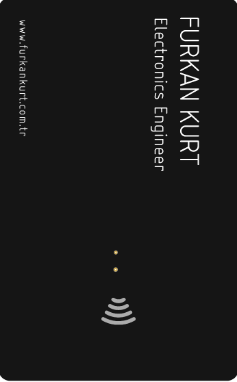
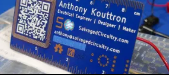
Silkscreen and Aesthetics
- Add your name, logo, and contact information
- Use contrasting colors for text (white on green, black on white, etc.)
- Include instructions like “Tap with NFC phone”
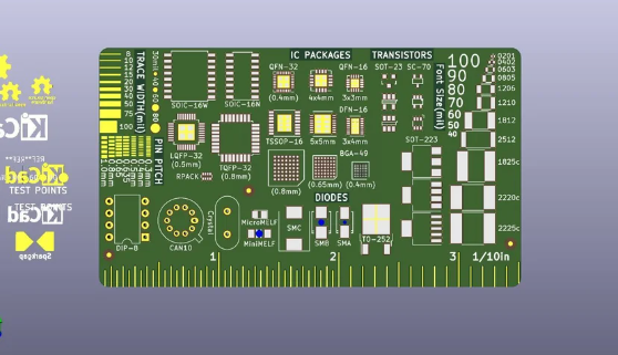
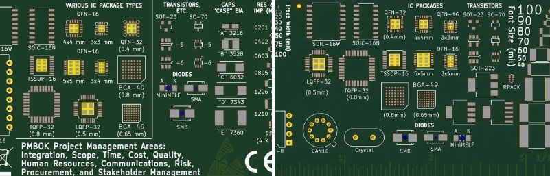
Manufacturing Considerations
- Clearances: Maintain at least 0.2mm spacing between copper features
- Holes: Minimum drill size is typically 0.3mm
- Text: Keep silkscreen text at least 1mm tall for readability
Fabrication Process
Ordering PCBs
Popular low-cost PCB manufacturers suitable for business cards:
- JLCPCB: Economical, fast turnaround
- PCBWay: Good quality, various finishing options
- OSH Park: U.S.-based, high-quality purple boards
Typical options to select:
- Layer count (1 or 2)
- Thickness (0.8mm, 1.0mm, or 1.6mm)
- Surface finish (HASL, ENIG, or immersion silver)
- Silkscreen color
- Solder mask color (black, white, and transparent are popular)
Assembly Options
- Manual assembly:
- Hand-solder NFC chip and components
- Requires fine-pitch soldering skills
- PCB assembly service:
- Many manufacturers offer assembly
- Requires providing component specifications
Programming the NFC Tag
Before final assembly, program your NFC chip using:
- Android apps:
- NFC Tools (most popular)
- TagWriter by NXP
- Desktop tools:
- ACS NFC Tag Manager
- NFCopy (Linux)
Common data formats to program:
- vCard: For contact information
- URL: For website links
- Plain text: For custom messages
- WiFi config: For network credentials
Advanced Features
LED Indicators
Add visual feedback when the card is scanned:
- Harvest energy from the NFC field to power LEDs
- Simple circuit: Connect LED with resistor across antenna
- Advanced versions: Use a charge pump to store energy
Multiple NFC Chips
Incorporate several NFC tags for:
- Different contact profiles
- Multiple website links
- Interactive experiences (scan different areas)
Embedded Microcontrollers
For truly interactive cards, add:
- Low-power MCUs like ATtiny85
- Energy harvesting circuits
- Programmable behaviors based on scan patterns
Testing and Troubleshooting
Common Issues
- Short read range:
- Check antenna tuning
- Verify proper chip connection
- Ensure no metal objects nearby
- Inconsistent performance:
- Test with multiple phones
- Check for proper grounding
- Verify programming was successful
Testing Methodology
- Range test: Measure maximum readable distance
- Compatibility test: Try with various phone models
- Data integrity: Verify stored information after multiple scans
Cost Analysis
Typical costs for a basic NFC PCB business card:
- PCB fabrication: $5-$20 for 10-100 units
- NFC chips: $0.50-$2 each
- Assembly: $0 if DIY, $10-$50 for professional assembly
- Shipping: Varies by location and speed
For 100 units, expect to pay $100-$300 total ($1-$3 per card).
Practical Applications
Beyond personal business cards, NFC PCB cards can serve as:
- Product authentication tags
- Interactive marketing materials
- Secure access cards
- Digital business card alternatives
Conclusion
Creating an NFC-enabled PCB business card combines electrical engineering, industrial design, and digital networking into one innovative professional tool. While the process involves multiple steps—from antenna design to PCB layout to programming—modern tools and manufacturing services make it accessible even to hobbyists. The result is a durable, conversation-starting business card that bridges the physical and digital worlds, demonstrating technical proficiency while providing practical contact information in a memorable format.
As NFC technology becomes increasingly ubiquitous in smartphones and other devices, these smart business cards represent the future of professional networking—where a simple tap can replace the exchange of paper cards while enabling richer, more interactive connections between professionals.