How to set the line width and line spacing of PCB
I believe that when you are designing PCB, you will find that wiring is indispensable, and the rationality of wiring also determines the aesthetics of PCB and the production cost. At the same time, it can also reflect the circuit performance and heat dissipation performance, as well as whether the performance of the device can be optimized.
In the previous article, the editor mainly shared some design rules for PCB line width and line spacing. In this article, we will give you a comprehensive summary of the wiring method of PCB, hoping to help you develop good design habits.
1.The wiring length should include the length of the via and the package pad.
2.The wiring angle is preferably 135°. Any angle will cause process problems in plate making.
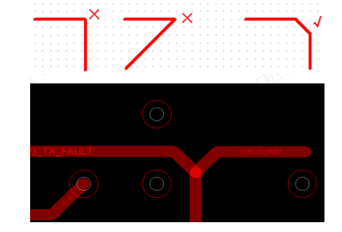
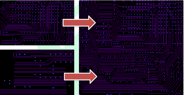
3.Avoid right-angle or sharp-angle wiring, which will cause the line width and impedance at the corner position to change, causing signal reflection, as shown in the figure below.
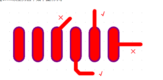
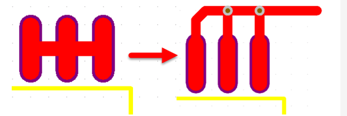
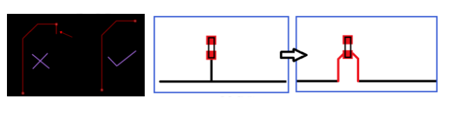
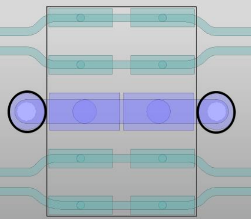
4.The wiring should be extended from the long direction of the pad, and avoid extending from the wide direction or the four corners of the pad. The corner of the wiring should be more than 6mil away from the pad position, as shown in the figure below.
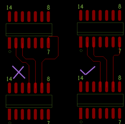
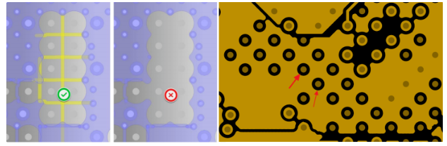
5.As shown in the figure below, adjacent pads are in the same network and cannot be directly connected. They need to be connected first and then connected. Direct connection is easy to tin during manual soldering.
6.For small CHIP devices, pay attention to the symmetry of the wiring and keep the wiring line width of the two ends consistent. For example, if one pin is copper-plated, the other pin should also be copper-plated as much as possible to reduce the drift and rotation of the device after the component is mounted, as shown in the figure below.
9bd3a260-2fff-11ee-9e74-dac502259ad0.png
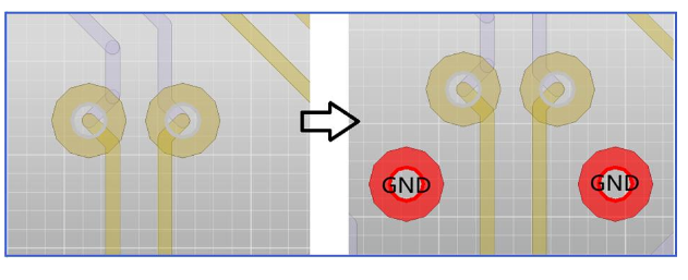
7.For signals with grounding requirements, the integrity of the grounding must be ensured, and GND holes should be drilled on the grounding line as much as possible. The distance between the two GND holes should not be too far, and should be kept at about 50-150mil, as shown in the figure below.
8.The routing should have a complete and continuous reference layer plane to avoid high-speed signal cross-zone. It is recommended that the high-speed signal be at least 40mil away from the edge of the reference plane, as shown in the figure below.
9.Since the surface mount device pad will cause impedance reduction, in order to reduce the impact of impedance mutation, it is recommended to dig out a reference layer according to the size of the pad directly below the surface mount pad. Commonly used surface mount devices include: capacitors, ESD, common mode suppression inductors, connectors, etc., as shown in the figure below.
10.As shown in the figure below, the loop area formed by the signal line and its loop should be as small as possible. The smaller the loop area, the smaller the external radiation and the less interference received from the outside world.
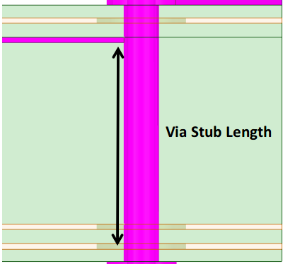
11.As shown in the figure below (above), STUB is not allowed in the wiring. The length of the stub should be minimized as much as possible during wiring. It is recommended that the stub length be zero. And avoid the via stub effect, especially when the stub length exceeds 12mil. It is recommended to evaluate the impact of the via stub on signal integrity through simulation, as shown in the figure below (below).
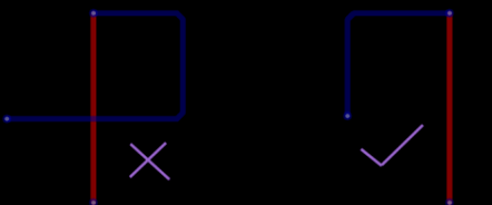
12.Try to avoid self-loops on different layers. This problem is prone to occur in multi-layer board design, and self-loops will cause radiation interference. As shown in the figure below.
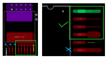
13.It is recommended not to place test points on high-speed signals.
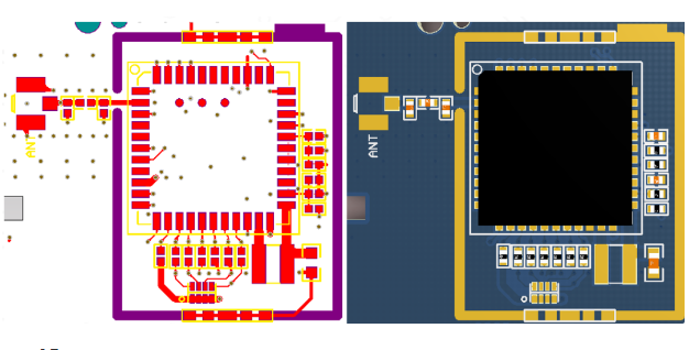
14.For signals that may cause interference or are sensitive (such as RF signals), a shielding cover must be planned. The width of the shielding cover is generally 40mil (generally kept above 30mil, which can be confirmed with the customer manufacturer). Try to make as many GND vias on the shielding cover as possible to increase its welding effect.
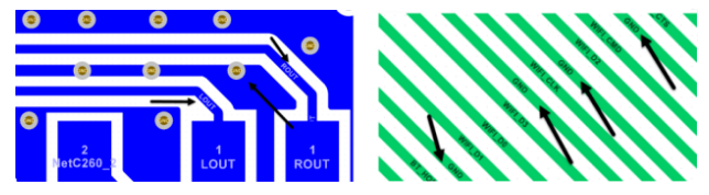
15.The wiring width of the same network should be consistent. The change of line width will cause uneven characteristic impedance of the line, and reflection will occur when the transmission speed is high. Under certain conditions, such as the structure of the connector lead-out line and the lead-out line of the BGA package, the change of line width may not be avoided due to the small spacing. The effective length of the inconsistent part in the middle should be minimized as shown in the figure below.

16.The line width of the IC pin lead should be less than or equal to the pad width, and the line width cannot be larger than the pad width. For some signals with wider line width due to current carrying requirements, the wiring can be kept consistent with the pin width first, and the line width can be thickened about 6-10mil after the wiring leads out of the pad, as shown in the figure below.
17.The wiring must be connected to the pad and the center of the via.
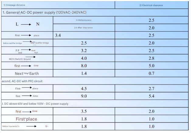
18.There is a high voltage signal, and its creepage distance must be guaranteed. The specific parameters are shown in the figure below.
19
If the design contains multiple DDR or other memory chips, the wiring topology must be confirmed with the customer to confirm whether there is a reference document.
20.The gold finger area needs to be windowed. When designing a multi-layer board, the copper of all layers below the gold finger should be hollowed out. The distance between the hollowed copper skin and the board frame is generally more than 3mm.
21.The wiring should plan the channel conditions at the bottleneck position in advance and reasonably plan the wiring capacity at the narrowest part of the channel.
22.The coupling capacitor should be placed as close to the connector as possible.
23.The series resistor should be placed close to the transmitting device, and the termination resistor should be placed close to the end. For example, the series resistor on the eMMC clock signal is recommended to be placed close to the CPU side (within 400mil).
24.It is recommended to drill a ground through hole on each ground pad of the IC (such as eMMC particles, FLASH particles, etc.) to effectively shorten the return path, as shown in the figure below.

25.It is recommended to drill a ground via for each ground pad of the ESD device, and the via should be as close to the pad as possible, as shown in the figure below.
26
Avoid wiring around clock devices (such as crystals, crystal oscillators, clock generators, clock distributors), switching power supplies, magnetic devices, plug-in vias, etc.
27
When the routing changes layers and the reference layer before and after the layer change is the ground plane, it is necessary to place a companion via next to the signal via to ensure the continuity of the return path. For differential signals, the signal vias and return vias should be placed symmetrically, as shown in the figure below (above); for single-ended signals, it is recommended to place a return via next to the signal via to reduce crosstalk between vias, as shown in the figure below (below).

28
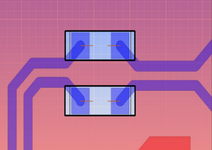
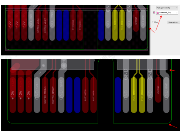
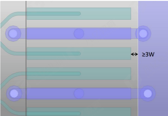
The distance between the ground copper foil of the connector and the signal PAD should be at least 3 times the line width, as shown in the figure below.
29
Use traces to connect the BGA area where the plane is disconnected, or perform plate cutting to avoid damaging the integrity of the plane, as shown in the figure below.
30
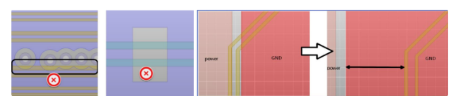
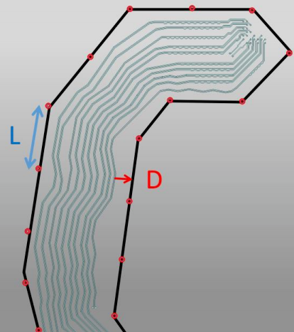
When PCB wiring needs grounding, the recommended grounding method is as follows, as shown in the figure below, L is the ground via spacing of the grounding wire; D is the spacing between the grounding wire and the signal line, which is recommended to be ≥4*W.
31
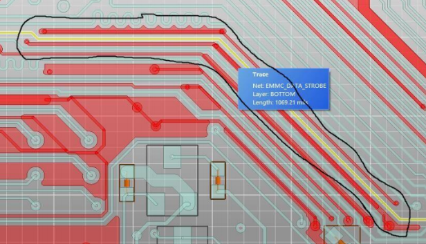
Some important high-speed single-ended signals, such as clock signals, reset signals, etc. (such as emmc_clk, emmc_datastrobe, RGMII_CLK, etc.) are recommended to be grounded. At least one ground hole should be drilled every 500mil of the grounding wire, as shown in the figure below.