How to identify the number of layers of a PCB circuit board
How to identify the number of layers of a PCB circuit board
It is worth noting that the reduction in the number of PCB layers can greatly save costs, and the price difference is very large. It can almost be said that the cost doubles for every two layers of PCB layers. That is to say, the cost of a four-layer PCB is twice that of a two-layer PCB, and the cost of a six-layer PCB is twice that of a four-layer PCB, and so on. The most luxurious Gigabyte EX58-EXTREME currently uses a 12-layer PCB, so its price is also very expensive.
The use of PCBs with fewer layers has a very huge effect on cost control. More importantly, most of the current DIYers have not yet put the number of PCB layers on the same level as video memory and GPU. In addition, the production of PCBs is generally designed by chip manufacturers or more powerful manufacturers and handed over to a PCB factory for OEM. The design of the PCB determines how to route and place components in the later stage, which is also a very advanced technology.
For DIYers, how do we choose a product with full materials? I believe that through this article, we can be of great help to everyone. In any case, judging the number of layers of a PCB is a skill that must be mastered. Here we will introduce several methods for judging the number of layers of a PCB.
First, visual inspection.
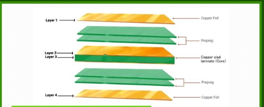
Since the layers in the PCB are tightly combined, it is generally not easy to see the actual number, but if you carefully observe the faults of the board, you can still distinguish them. If you are careful, we will find that there is one or several layers of white material in the middle of the PCB. In fact, this is the insulation layer between the layers, which is used to ensure that there will be no short circuit between different PCB layers. Because the current multi-layer PCB boards use more single- or double-sided wiring boards, and put an insulation layer between each layer of the board and then press it together, the number of layers of the PCB board represents how many independent wiring layers there are, and the insulation layer between the layers has become the most intuitive way for us to judge the number of layers of the PCB.
Second, the guide hole and blind hole light method.
The guide hole light method uses the “guide hole” on the PCB to identify the number of PCB layers. The principle is mainly because the circuit connection of the multi-layer PCB uses the guide hole technology. If we want to see how many layers the PCB has, we can identify it by observing the guide hole.
On the most basic PCB (single-sided motherboard), the parts are concentrated on one side, and the wires are concentrated on the other side. If you want to use a multi-layer board, you need to punch holes in the board so that the component pins can pass through the board to the other side, so the guide holes will penetrate the PCB board. Therefore, we can see that the pins of the parts are soldered on the other side.
For example, if the board uses a 4-layer board, it is necessary to route on the 1st and 4th layers (signal layers), and the other layers have other uses (ground layer and power layer). The purpose of placing the signal layer on both sides of the power layer and the ground layer is to prevent mutual interference and facilitate correction of the signal line. If some board guide holes appear on the front of the PCB board, but cannot be found on the back, then it must be a 6/8-layer board. If the same guide holes can be found on both sides of the PCB board, it is naturally a 4-layer board.
However, many board manufacturers currently use another routing method, which is to connect only some of the lines, and use buried and blind hole technology in the routing. Blind vias connect several layers of internal PCB to the surface PCB without penetrating the entire circuit board.
Buried vias only connect the internal PCB, so they cannot be seen from the surface alone. Since blind vias do not need to penetrate the entire PCB, if there are six layers or more, the light will not pass through when the board is facing the light source. Therefore, there was a very popular saying before: judge whether the PCB is four-layer or six-layer or more by whether the vias leak light. This method has its reasons, but it is also not applicable. It can be used as a reference method.
Third, the accumulation method.
To be precise, this is not a method, but an experience. However, this is what we think is the most accurate. We can judge the number of layers of the PCB by the routing and component positions of some public board PCB boards. Because in the current IT hardware industry where the update is so fast, there are not many manufacturers who have the ability to redesign the PCB.
For example, a few years ago, a large number of 9550 graphics cards used 6-layer PCB design. Careful friends can compare how much difference there is between it and the 9600PRO or 9600XT board type? Only some components are omitted, and the PCB is highly consistent.
In the 1990s, there was a popular saying that the number of PCB layers can be seen by placing the PCB vertically, and many people believed it. This statement was later proved to be nonsense. Even if the manufacturing process at that time was backward, how could the eyes distinguish the distance thinner than a hair? Later, this method continued and modified, and gradually evolved into another measurement method. Now many people believe that the number of PCB layers can be measured with precision measuring instruments such as “vernier calipers”, and we dare not agree with this statement.
Regardless of whether there is such a precision instrument, why can’t we see that the 12-layer PCB is 3 times thicker than the 4-layer one? Different PCBs will use different manufacturing processes, and there is no unified standard for measurement. How to judge the number of layers based on thickness?
In fact, the number of PCB layers has a great impact on the board. For example, why should at least 6-layer PCB be used to install dual CPUs? Because this allows the PCB to have 3 or 4 signal layers, 1 ground layer, and 1 or 2 power layers. Then the signal lines can be far enough apart to reduce interference with each other and have sufficient current supply. However, it is completely sufficient for general boards to use 4-layer PCB design. Using 6-layer PCB is too wasteful of cost and does not improve performance.
The more layers of PCB multilayer boards, the better?
Now PCB is very common in life. PCB board is an important carrier of large-scale integrated circuits. There was a misunderstanding in the DIY industry before: “The more layers of PCB, the better”, but it is not the case. Increasing the number of PCB layers is actually a helpless move. Due to the limitation of size, double-sided wiring cannot meet the demand, so more layers of PCB boards are needed to support it. The cost of multi-layer PCB is higher and it is not conducive to making more cost-effective products.
Generally, there is this to identify how many layers of PCB
With the advancement of technology, the integration of electronic components is getting higher and higher, the number of layers of motherboard PCB has gradually decreased, and the materials that need to be “stacked” have also begun to be highly integrated. Think about the previous TV sets that needed a “hot” volume, and now LCD TVs have been very thin and have better display effects (ignoring the difference between cathode ray tube and liquid crystal technology here), and the same is true for the DIY industry.
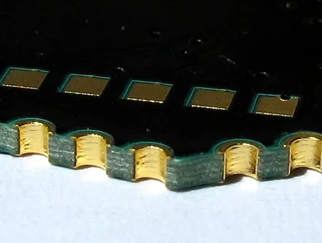
The side view of an excellent PCB
The materials of PCBs are different. At present, the mainstream PCBs all use glass fiber as the main raw material. The identification method is very simple. If the side is very flat and not rough, it is a relatively good PCB. If you see a particularly rough PCB that may be made of fire-resistant cardboard, please use this motherboard to slap the store’s face (you will bear all legal consequences caused by this action, and the author is not prepared to take any responsibility). I’m sorry that I didn’t find a side view photo of the fire-resistant cardboard PCB.
Click to view the side view of the motherboard PCB
Oh, by the way, a good PCB board is not necessarily particularly hard, but it must be very tough, and it can quickly return to its original state after being gently bent, without brittle cracks and deformation. Of course, if you have a lot of strength, the author does not recommend that you use this method to test the strength of the motherboard, which is easy to cause damage beyond the free warranty.