Analysis of PCB Trace Breakage Causes
Abstract
Printed Circuit Boards (PCBs) are fundamental components in modern electronics, providing mechanical support and electrical connectivity. However, PCB trace breakage is a common issue that can lead to device failure. This paper examines the primary causes of PCB trace breakage, including manufacturing defects, mechanical stress, environmental factors, and design flaws. By understanding these causes, engineers can implement preventive measures to enhance PCB reliability.
1. Introduction
PCB trace breakage refers to the physical separation or cracking of conductive pathways on a PCB, disrupting electrical signals. Such failures can result in intermittent connections or complete circuit failure. Identifying the root causes of trace breakage is essential for improving PCB design, manufacturing, and application in harsh environments.
2. Manufacturing Defects
Manufacturing defects are among the most common causes of PCB trace breakage. These defects can occur during etching, plating, or lamination processes.
2.1 Over-Etching or Under-Etching
- Over-Etching: Excessive chemical etching can thin out copper traces, making them more susceptible to breakage under mechanical stress.
- Under-Etching: Insufficient etching leaves residual copper, potentially causing short circuits, but may also weaken trace adhesion.
2.2 Poor Plating Quality
- Voids in Plating: Inadequate electroplating can create voids or weak spots in through-holes and vias, leading to fractures under thermal or mechanical stress.
- Uneven Copper Deposition: Inconsistent copper thickness can result in weak traces prone to cracking.
2.3 Delamination and Layer Misalignment
- Delamination: Poor bonding between PCB layers can cause separation, stressing traces and leading to breakage.
- Layer Misalignment: Misaligned layers during lamination can create uneven stress distribution, weakening traces.
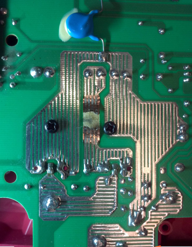
3. Mechanical Stress
Mechanical forces during assembly, handling, or operation can cause PCB trace fractures.
3.1 Flexing and Bending
- Excessive Flexing: PCBs used in flexible applications (e.g., wearables) may experience repeated bending, leading to metal fatigue and trace cracks.
- Improper Handling: Rough handling during assembly or installation can induce micro-cracks in traces.
3.2 Vibration and Shock
- High-Vibration Environments: PCBs in automotive or industrial applications may suffer from vibration-induced stress, causing gradual trace deterioration.
- Impact Shock: Sudden impacts (e.g., drops) can fracture traces, especially near connectors or mounting holes.
3.3 Improper Soldering Techniques
- Thermal Stress from Soldering: Excessive heat during soldering can weaken traces, especially thin ones.
- Mechanical Stress from Components: Heavy or poorly mounted components can exert stress on adjacent traces.
4. Environmental Factors
External environmental conditions can accelerate PCB trace degradation.
4.1 Thermal Cycling
- Repeated Expansion/Contraction: Temperature fluctuations cause PCB materials (e.g., FR4) and copper traces to expand and contract at different rates, leading to stress fractures.
- High-Temperature Exposure: Prolonged exposure to high temperatures can anneal copper, making it brittle.
4.2 Moisture and Corrosion
- Electrochemical Migration: Moisture ingress can lead to dendritic growth, causing short circuits and trace corrosion.
- Oxidation: Exposed copper traces may oxidize, weakening conductivity and structural integrity.
4.3 Chemical Exposure
- Harsh Chemicals: PCBs exposed to acids, solvents, or industrial chemicals may experience trace corrosion.
5. Design-Related Causes
Poor PCB design can increase the likelihood of trace breakage.
5.1 Insufficient Trace Width
- High-Current Applications: Thin traces carrying excessive current can overheat and break.
- Manufacturing Limitations: Traces narrower than the manufacturer’s capability may be inconsistently etched.
5.2 Sharp Corners and Acute Angles
- Stress Concentration: 90-degree turns or acute angles in traces create stress points, increasing fracture risk.
- Current Density Issues: Sharp corners can lead to uneven current distribution, causing localized heating.
5.3 Poor Via Placement
- Microvia Cracking: High-density vias in rigid-flex PCBs may crack under stress.
- Thermal Stress Around Vias: Uneven thermal expansion can weaken via connections.
6. Prevention and Mitigation Strategies
To minimize PCB trace breakage, engineers should:
- Optimize Manufacturing Processes: Ensure proper etching, plating, and lamination.
- Enhance Mechanical Durability: Use thicker copper, flexible substrates, or strain relief features.
- Improve Environmental Protection: Apply conformal coatings or use moisture-resistant materials.
- Follow Design Best Practices: Avoid sharp corners, ensure adequate trace width, and optimize via placement.
7. Conclusion
PCB trace breakage can result from manufacturing defects, mechanical stress, environmental exposure, or design flaws. By identifying these causes, engineers can implement corrective measures to enhance PCB reliability. Future advancements in materials and manufacturing techniques will further reduce trace breakage risks.