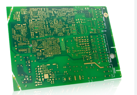
Why does PCB need 20H principle?
1) In PCB design, small power supply should be copper-plated on the signal layer first, and then connected by routing that can carry current;
2) In PCB design, if 12V and 5V power supply is the input power supply of switching power supply, it should be processed on the signal layer (surface layer and inner layer signal layer). If it must be split on the plane layer, it should not be used as the reference plane of important signal lines; this can effectively reduce the impact of such “high” voltage on the signal;
3) In PCB design, if the split power plane is used as the reference plane of the signal, the power plane should be used as the signal reference plane of the power module first; if there are multiple power supplies, the power supply with low voltage should be used first; for example, DDR3 uses 1.5V power supply, then the 1.5V power plane can be used as the signal reference plane of DDR3 module, but try not to refer to 3.3V power supply or other power supplies; (usually DDR3 data references the ground plane, and address control signal references the power plane)
4) The power plane and ground plane of PCB design are closely adjacent. If the power plane is adjacent to the signal layer, try to add more GND copper on the signal layer and drill GND vias;
5) The width of the dividing line in PCB design should be reasonable; the width of the dividing line is related to the voltage difference between the two power supplies. Generally, it is recommended that the dividing width between analog and digital is 25mil; the dividing width between digital is 15mil, which can be smaller locally; the dividing line width can also be flexibly adjusted according to the space on the board. In principle, the larger the better;
6) The width of the chassis ground separation isolation of PCB design is preferably 2mm, and it is adjusted locally according to the situation. Generally, it is required to be not less than 1mm; other signals are kept away from the chassis ground, including signal lines, vias, copper plating, etc.;
7) If the power/ground plane is divided in PCB design, pay attention to the adjacent signal layer signal lines not to cross the division, and try to avoid the crossing of high-speed signals on the divided reference plane.
8) The power vias of the PCB design should avoid the isolation belt, and the isolation belt should avoid copper, which will cause such power vias to be unconnected;
9) In the power supply of the analog area of the PCB design, in order to reduce the impact of the power supply on the signal, it is generally not recommended to lay the power network copper in a large area. It is generally processed on the signal layer. The power supply copper or routing can meet the current carrying capacity. In other areas, as much ground copper and ground vias as possible;
10) The high-voltage power supply and low-voltage power supply of the PCB design should be divided into zones, and the larger the spacing, the better; avoid high voltage interference with low-voltage power supply and signals;
11) Common creepage avoidance spacing in PCB design:
i. When the voltage is less than 24V, the surface cover solder mask and the spacing ≥0.1 3mm; the surface is not covered with solder mask, and the spacing is ≥0.64mm
ii. When the voltage is 24V≤<48V, the spacing on the primary side is ≥0.5mm, and the spacing on the secondary side is ≥0.2mm;
iii. When the voltage is 48V≤<100V, the spacing is ≥1mm
iv. When the voltage is 100V≤<200V, the spacing is ≥1.5mm
v. When the voltage is 200V≤<400V, the spacing is ≥2.5mm
vi. When the voltage is 400V≤<600V, the spacing is ≥3.2mm
vii. When the voltage is ≥600V, the spacing is ≥5mm
12) PCB design confirms that the power supply and ground can carry enough current. Does the number of vias meet the load requirements?
(Estimation method: 1A/mm line width when the outer copper thickness is 1oz, and 0.5A/mm line width for the inner layer)
13) In order to reduce the edge radiation effect of the plane in PCB design, the 20H principle should be met as much as possible between the power layer and the ground layer.
(If conditions permit, the more the power layer is indented, the better).
“20H principle” means to ensure that the edge of the power plane is indented at least 20 times the distance between the two planes than the edge of the ground plane (0V reference plane), where H refers to the distance between the power plane and the ground plane, as shown in the figure below.
Why is the 20H principle needed?
In high-speed PCBs, the mutual coupling of RF energy between the power plane and the ground plane usually becomes an edge flux leakage, and the RF energy (RF current) will radiate along the edge of the PCB. In order to reduce this coupling effect, the physical size of all power planes must be 20H smaller than the size of the nearest ground plane.
14) If there is ground segmentation in the PCB design, check whether the ground to avoid segmentation does not form a loop?
15) Do the power planes of different adjacent layers in the PCB design avoid overlapping?
16) Is the isolation of the PCB design protection ground and GND greater than 4mm?
17) Is the PCB design near the connector panel equipped with a 10~20mm protection ground, and is the layer connected with double-row staggered holes?
18) Check the effective width of the power trace in the PCB design: Is there any interruption in the positive and negative copper sheets (BGA, dense vias, and whether there is a high-speed bus in the dense vias), and pay special attention to 0.8mmBGA.