PCB Characteristics and PDN Performance
Basic design rules for power distribution networks (PDNs) tell us that the best performance comes from a consistent, frequency-independent (or flat) impedance profile. This is one reason why power supply stability is important, because a poorly stable source will result in impedance peaks that degrade the flat impedance profile and the performance of the powered circuit.
Since no impedance path is perfectly flat, some design adjustments are needed. This article aims to help you make some compromises that will have the least impact on system performance.
The source impedance should match the transmission line impedance.
This is the basic premise of S-parameter measurements and all RF devices in general. The source impedance (most commonly 50Ω) is connected to a coaxial cable with impedance matching the source, and the load is also terminated to the same impedance. This practice achieves perfectly flat impedance, which is consistent whether the source sees the load or the load sees the source.
The output impedance of the regulator can be thought of as a source, and the PCB layer can be thought of as a transmission line. The back-end decoupling capacitor is the load.
Transmission Line Basics
When the frequency is below the transmission line resonant frequency, the transmission line characteristic impedance can be defined by inductance and capacitance terms. Capacitance can be measured when the far end of the transmission line is unterminated. Inductance can be measured when the far end of the transmission line is shorted. The characteristic impedance of the transmission line is determined by these two measurements, namely:
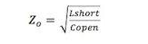
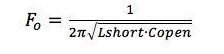
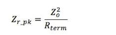
The frequency at the intersection of the inductance and capacitance is the characteristic impedance, which is equal to:
A properly matched transmission line presents a completely flat impedance curve with an amplitude equal to the characteristic impedance. An improperly terminated transmission line behaves either capacitively or inductively, producing many resonant and anti-resonant frequencies at multiples of the transmission line resonant frequency. If the transmission line is capacitive, then the anti-resonance occurs first. If the transmission line is inductive, then the resonance occurs first. In both cases, the frequency of the first resonance or anti-resonance is:
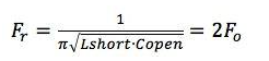
Figure 1 shows these relationships using a 50Ω coaxial cable simulation. The unterminated terminal impedance was measured with the cable end open, shorted, and matched.
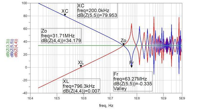
Figure 1: Transmission line near-end impedance open (blue), shorted (red), and properly matched (green), another interesting relationship.
In the case of a mismatch between the transmission line and the source, there are two possible solutions, depending on whether the termination resistor is greater than or less than the characteristic impedance. If the termination resistor is less than the characteristic impedance of the transmission line, then the anti-resonance peaks will exceed the termination resistor. These impedance peaks are defined as:
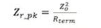
The resonance minimum is equal to the termination resistor.
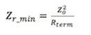
If the termination resistor is greater than the characteristic impedance of the transmission line, then the resonance peak is equal to the termination resistor. The anti-resonance minimum is defined as:
These relationships can be shown using the previous simulation model with termination resistors of 24.9Ω and 210Ω, respectively, which are matched in Figure 2.
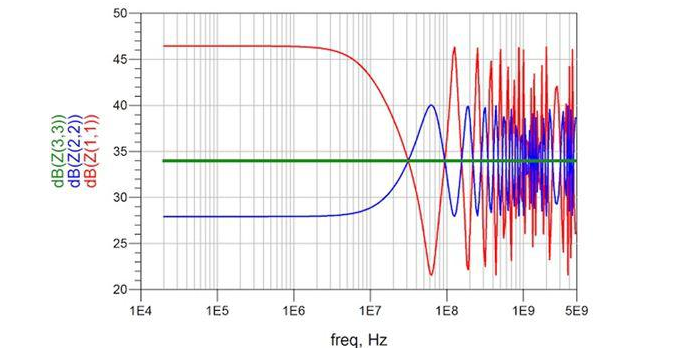
Figure 2: Transmission line unterminated with terminal impedances of 24.9Ω (blue), 210Ω (red), and properly matched (green).
These relationships are confirmed in Figure 3 with measurements of 50Ω coaxial cables terminated with 24.9Ω and 210Ω.
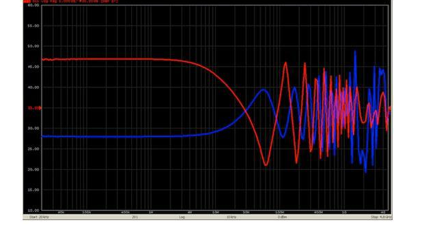
Figure 3: Measurement results of 50Ω coaxial cables terminated with 210Ω (red) and 24.9Ω (blue).
These concepts are extended to an actual double-sided printed circuit board with an SMA connector soldered to the center of a 4.5″ x 6.3″ bare copper clad PCB, as shown in Figure 4.
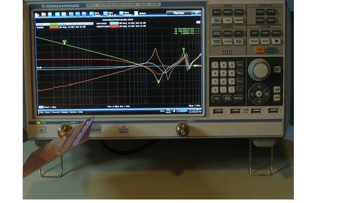
Figure 4: The open (green) and short (orange) impedances of a 4.5″ x 6.3″ double-sided copper clad PCB with an SMA connector on one side. The impedance is also measured with 2.7Ω (blue) and 10Ω (red) termination resistors directly opposite the SMA connector.
The resistors are connected to the PCB with very short braids to minimize interconnect inductance.
We can approximate the characteristic impedance of the PCB using the oscilloscope measurements in Figure 4. The capacitance is estimated using the marker M3.
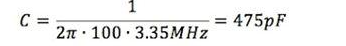
The capacitance is estimated using the 70MHz, 10dBΩ point.
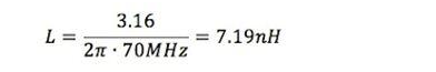
Using (1), the characteristic impedance can be calculated as:
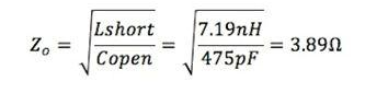
Alternatively, the characteristic impedance can be viewed as the intersection of the open and short impedances, which occurs at approximately 11.5dBΩ or 3.76Ω. The characteristic impedance of the PCB can also be calculated using (4) and the approximate peak impedance (14.5dBΩ) with a 2.7Ω termination resistor.
Re-transform and calculate Zo.

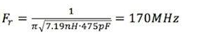
The first resonant frequency or anti-resonant frequency can be calculated using (3), namely:
The measurement is repeated with a 3.6Ω termination resistor, as shown in Figure 5.
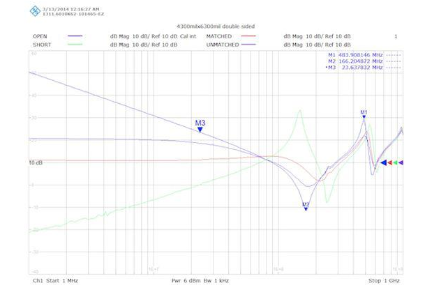
Figure 5: The same PCB is measured with a 3.6Ω termination resistor instead of a 2.7Ω termination resistor (red). Note that with a 3.6Ω termination resistor, there are only a few peaks indicating that the characteristic impedance is slightly greater than 3.6Ω.
The PCB is simulated and compared to Figure 5, and the results are shown in Figure 6.
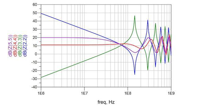
Figure 6: The PCB simulation results are compared to the measured results shown in Figure 5.
Finally, the dynamic transient response is simulated at the PCB resonant frequency using 0.6Ω and 3.6Ω source impedances at the power supply end. The simulation model is shown in Figure 7 and the simulation results are shown in Figure 8.
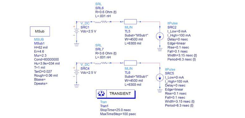
Figure 7: Dynamic load transient ADS simulation at the resonant frequency using 0.6Ω and 3.6Ω source impedances to represent the regulator output impedance.
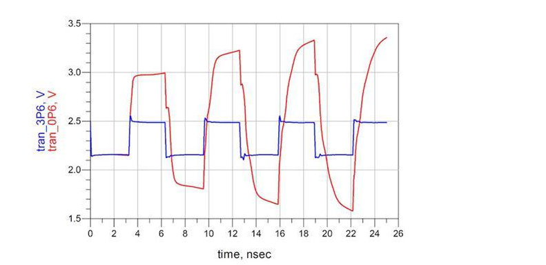
Figure 8: Transient response simulation results show that the transient response of the lower 0.6Ω source resistor (red) has a much larger voltage excursion than the matched 3.6Ω source resistor (blue).
Conclusion
This article discusses several methods for determining the characteristic impedance of the board and defines the important relationship between PCB characteristics and PDN performance using simulation models. The relationship is confirmed after actual measurements.
It can be determined whether the PCB impedance is greater or less than the termination impedance by observing whether the first defect is a resonant point or an anti-resonant point, and whether the termination impedance is greater than the PCB impedance.
These results clearly show that in order to optimize PDN performance, the PCB layer impedance must be matched to the output impedance of the regulator. It is best to make the PCB layer impedance equal to the output impedance of the regulator. If this is not possible, the PCB impedance should be lower than the regulator output impedance to better contain the peak excursion associated with the peak impedance maximum.