Impedance Control in PCB Manufacturing: A Detailed Analysis
1. Introduction
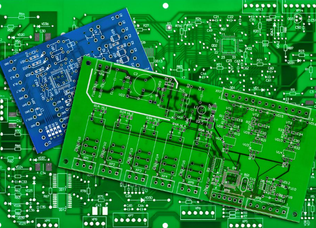
Printed Circuit Boards (PCBs) are the backbone of modern electronics, enabling the interconnection of components in devices ranging from smartphones to aerospace systems. As signal frequencies increase and devices become more compact, maintaining signal integrity is critical. One of the most crucial aspects of signal integrity is impedance control, which ensures that signals propagate efficiently without distortion or reflection.
This article provides an in-depth analysis of impedance control in PCB manufacturing, covering fundamental concepts, design considerations, manufacturing processes, and testing methodologies.
2. Fundamentals of Impedance in PCBs
2.1 What is Impedance?
Impedance (Z) is the opposition that a circuit presents to alternating current (AC). In PCBs, it is primarily determined by the inductance (L), capacitance (C), and resistance (R) of the transmission lines. For high-speed signals, characteristic impedance (typically 50Ω, 75Ω, or 100Ω in differential pairs) must be tightly controlled to prevent signal degradation.
2.2 Why is Impedance Control Important?
- Signal Integrity: Mismatched impedance causes reflections, leading to signal distortion.
- EMI Reduction: Proper impedance matching minimizes electromagnetic interference (EMI).
- High-Speed Performance: Ensures reliable data transmission in high-frequency applications (e.g., DDR, PCIe, USB).
2.3 Types of Impedance in PCBs
- Single-Ended Impedance – The impedance of a single trace relative to a reference plane.
- Differential Impedance – The impedance between two paired traces carrying complementary signals.
- Common-Mode Impedance – The impedance seen by common-mode signals in differential pairs.
3. Key Factors Affecting PCB Impedance
3.1 Trace Geometry
- Width (W): Wider traces reduce impedance, while narrower traces increase it.
- Thickness (T): Thicker copper increases capacitance, lowering impedance.
- Spacing (S): Affects coupling in differential pairs.
3.2 Dielectric Material Properties
- Dielectric Constant (Dk or εr): Lower Dk materials (e.g., Rogers, PTFE) provide better high-frequency performance.
- Loss Tangent (Df): Indicates signal loss; lower values (e.g., <0.005) are preferred for high-speed designs.
- Thickness (H): Thinner dielectrics reduce impedance.
3.3 Reference Planes
- A solid ground or power plane is essential for controlled impedance.
- Distance from the trace to the reference plane (H) impacts impedance.
3.4 Manufacturing Tolerances
- Etching Variations: Over-etching reduces trace width, increasing impedance.
- Layer Misalignment: Affects impedance consistency in multilayer PCBs.
- Surface Finish: ENIG, HASL, or immersion silver can slightly alter impedance.
4. PCB Design for Impedance Control
4.1 Stackup Design
A well-designed PCB stackup ensures consistent impedance:
- Symmetrical Layers: Prevents warping and maintains impedance uniformity.
- Controlled Dielectric Thickness: Critical for impedance matching.
- Proper Material Selection: FR-4 is common, but high-speed designs may require low-Dk materials.
4.2 Trace Routing Techniques
- Microstrip vs. Stripline:
- Microstrip: Trace on an outer layer with a single reference plane (easier to tune but more susceptible to noise).
- Stripline: Trace embedded between two reference planes (better shielding but harder to adjust).
- Differential Pair Routing: Maintain consistent spacing and length matching.
- Avoid Sharp Bends: Use 45° or curved traces to minimize impedance discontinuities.
4.3 Impedance Calculation Tools
- Field Solvers: Tools like Polar SI9000, Altium, and HyperLynx simulate impedance based on geometry and material properties.
- Manufacturer’s Guidelines: PCB fabricators provide impedance control specifications.
5. Manufacturing Process for Controlled Impedance
5.1 Material Selection
- Standard FR-4 for general applications.
- High-frequency laminates (e.g., Rogers, Isola) for RF/microwave PCBs.
5.2 Precise Etching and Plating
- Laser Direct Imaging (LDI): Ensures accurate trace patterning.
- Controlled Copper Plating: Maintains consistent trace thickness.
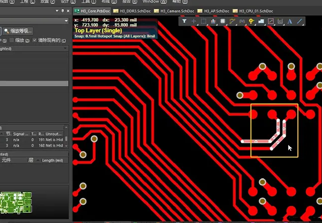
5.3 Layer Alignment
- Optical Alignment Systems: Ensure precise layer registration in multilayer PCBs.
- Automated Optical Inspection (AOI): Detects misalignment early.
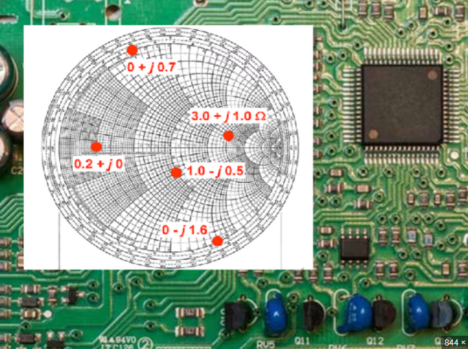
5.4 Impedance Testing
- Time-Domain Reflectometry (TDR): Measures impedance variations along traces.
- Network Analyzers: Validate high-frequency performance.
6. Testing and Validation
6.1 TDR Testing
- Sends a pulse and measures reflections to detect impedance mismatches.
- Provides impedance profiles along the trace.
6.2 Cross-Sectional Analysis
- Verifies trace dimensions and dielectric thickness.
- Ensures manufacturing compliance with design specs.
6.3 Signal Integrity Simulations
- Pre-layout and post-layout simulations identify potential issues.
- Tools: ANSYS HFSS, Keysight ADS, Cadence Sigrity.
7. Common Challenges and Solutions
7.1 Impedance Variations Due to Manufacturing Tolerances
- Solution: Work closely with PCB manufacturers to define acceptable tolerances.
7.2 High-Frequency Losses
- Solution: Use low-loss materials and optimize trace geometry.
7.3 Crosstalk in Dense Designs
- Solution: Increase spacing, use guard traces, or implement ground shielding.
8. Future Trends in PCB Impedance Control
- Advanced Materials: Development of ultra-low Dk/Df laminates.
- 5G and mmWave PCBs: Tighter impedance control for >10 GHz applications.
- Embedded Passive Components: Reducing parasitic effects for better impedance matching.
9. Conclusion
Impedance control is a critical aspect of PCB design and manufacturing, especially for high-speed and high-frequency applications. By understanding the factors affecting impedance—such as trace geometry, dielectric properties, and manufacturing processes—engineers can optimize PCB performance. Advanced simulation tools, precise fabrication techniques, and rigorous testing ensure that impedance-controlled PCBs meet the demands of modern electronics.
As technology evolves, the need for tighter impedance tolerances and innovative materials will continue to grow, making impedance control an essential discipline in PCB engineering.