High Multilayer PCB Production and Process Control
Abstract
This paper provides a comprehensive overview of high multilayer printed circuit board (PCB) production and the critical process controls required to ensure quality and reliability. As electronic devices become increasingly complex, the demand for high multilayer PCBs (typically 8-32 layers or more) has grown significantly. The manufacturing of these sophisticated boards presents numerous technical challenges that require precise process control at every stage. This article examines the complete production workflow, from material selection to final testing, highlighting key process parameters, common defects, and quality control measures. Special attention is given to lamination, drilling, plating, and registration control—processes that become increasingly critical as layer counts rise. The paper also discusses emerging trends in high multilayer PCB manufacturing and the process control technologies that enable these advancements.
1. Introduction
The evolution of electronic devices toward higher performance, smaller form factors, and increased functionality has driven the development of high multilayer printed circuit boards. These complex substrates, typically defined as having 8 or more conductive layers, enable the dense interconnections required by modern digital systems while maintaining signal integrity and power distribution characteristics.
High multilayer PCBs find applications in:
- High-performance computing systems
- Network infrastructure equipment
- Aerospace and defense electronics
- Medical imaging systems
- Advanced telecommunications hardware
Producing these boards requires exceptional process control due to:
- Increased likelihood of registration errors
- Greater susceptibility to delamination
- More complex impedance control requirements
- Challenging plating uniformity across thick stacks
- Higher incidence of drilling defects
This paper systematically examines the production process and identifies critical control points that determine final product quality.
2. Material Selection and Preparation
2.1 Base Materials
The foundation of any multilayer PCB begins with proper material selection. Key considerations include:
- Dielectric materials: High-performance FR-4, polyimide, or specialized low-loss materials
- Copper foil: Typically electrodeposited (ED) or rolled annealed (RA) copper with various surface treatments
- Prepreg: Resin-impregnated glass fiber that bonds core layers during lamination
For high layer counts, materials must exhibit:
- High glass transition temperature (Tg > 170°C)
- Low coefficient of thermal expansion (CTE)
- Excellent dimensional stability
- Consistent dielectric properties
2.2 Material Handling and Storage
Proper material control begins before production:
- Temperature and humidity-controlled storage (typically 20-25°C, 30-50% RH)
- FIFO (first-in-first-out) inventory management
- Baking procedures for moisture removal when required
3. Inner Layer Processing
3.1 Imaging and Etching
The process of defining inner layer circuits involves:
- Cleaning: Acidic or alkaline cleaners remove oxides and contaminants
- Lamination: Dry film resist application with controlled temperature, pressure, and speed
- Exposure: Precise alignment and UV exposure through phototool
- Development: Alkaline solution removes unexposed resist
- Etching: Ammoniacal or cupric chloride etchants define copper traces
- Strip: Removal of remaining resist
Critical controls:
- Exposure energy (typically 50-100 mJ/cm²)
- Etch rate and uniformity (maintaining 1:1 aspect ratio)
- Line width tolerance (usually ±10% of nominal)
3.2 Automated Optical Inspection (AOI)
100% inspection of inner layers detects:
- Opens and shorts
- Necking or bulging traces
- Etching defects
- Registration errors
Advanced systems use pattern matching algorithms with resolution down to 10μm.
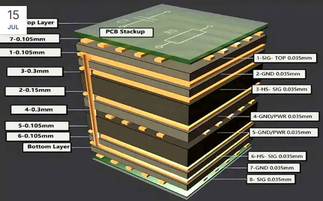
4. Lamination Process
4.1 Layup
The stacking of inner layers, prepreg, and copper foil requires:
- Precise layer-to-layer registration
- Controlled prepreg resin content (typically 42-52%)
- Proper bookending with steel plates
4.2 Lamination Cycle
A typical thermal pressure cycle includes:
- Initial press: 50-100 psi at room temperature
- Ramp: 2-5°C/min to 180-200°C
- Cure: 60-120 minutes at peak temperature
- Cool down: Controlled rate of 2-3°C/min
Critical parameters:
- Peak temperature (±2°C control)
- Pressure profile (typically 200-500 psi)
- Vacuum level (<5 Torr preferred)
- Ramp rates (affects resin flow)
4.3 Sequential Lamination
For very high layer counts (>16 layers), sequential lamination divides the stack into sub-composites that are later joined. This approach:
- Reduces registration errors
- Improves yield
- Allows for buried via structures
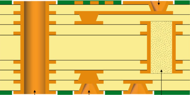
5. Drilling Process
5.1 Mechanical Drilling
High multilayer boards present drilling challenges due to:
- Increased stack thickness (may exceed 6mm)
- Mixed materials with different drilling characteristics
- Small via diameters (often 0.15-0.30mm)
Key controls:
- Spindle speed (80-150 krpm)
- Feed rate (1-5 m/min)
- Retract rate
- Hit count per drill bit (typically 500-2000 hits)
- Chip load (0.02-0.08mm/rev)
5.2 Laser Drilling
For microvias (<100μm), UV or CO₂ lasers provide:
- Higher precision
- Smother via walls
- No drill bit wear
Process controls include:
- Pulse energy
- Frequency
- Number of pulses
- Focus position
6. Plating Processes
6.1 Desmear and Etchback
Prepares hole walls for plating by:
- Removing drilling debris (desmear)
- Creating micro-roughness (etchback)
Methods:
- Chemical (permanganate)
- Plasma
- Laser
6.2 Electroless Copper
Provides initial conductive layer:
- Typically 0.3-1.0μm thickness
- Controlled deposition rate
- Uniform coverage
6.3 Electrolytic Plating
Builds up copper thickness (25-35μm):
- Acid copper sulfate baths
- Current density control (1-3 A/dm²)
- Solution agitation
- Temperature control (20-25°C)
Critical metrics:
- Throwing power (hole center vs. surface thickness)
- Uniformity across panel
- Ductility (important for thermal cycling)
7. Outer Layer Processing
7.1 Imaging
Similar to inner layers but with additional considerations:
- Tighter registration tolerances
- Thicker resists for plating
- Finer feature requirements
7.2 Pattern Plating
Adds copper and tin/lead or tin as etch resist:
- Copper: 20-30μm
- Tin: 5-10μm
7.3 Etching
Removes unwanted copper while preserving plated features:
- Typically alkaline ammonia or cupric chloride
- Critical control of undercut
8. Solder Mask and Surface Finish
8.1 Solder Mask Application
Protects copper and prevents bridging:
- Liquid photoimageable (LPI) most common
- Cured thickness 15-30μm
- Resolution to 50μm openings
8.2 Surface Finishes
Common options include:
- ENIG (Electroless Nickel Immersion Gold)
- Immersion Silver
- OSP (Organic Solderability Preservative)
- ENEPIG (for wire bonding)
Each requires specific process controls for thickness and composition.
9. Electrical Testing and Inspection
9.1 Electrical Testing
- Flying probe or fixture-based testing
- Continuity and isolation checks
- Impedance testing for critical nets
9.2 Final Inspection
- Visual examination
- Dimensional verification
- Microsection analysis for process validation
10. Process Control Methodologies
Effective manufacturing relies on:
10.1 Statistical Process Control (SPC)
- Control charts for key parameters
- Cp/Cpk analysis for capability
- Trend monitoring
10.2 Design of Experiments (DOE)
Used to optimize processes and understand parameter interactions.
10.3 Advanced Process Control
- Real-time monitoring with feedback loops
- Predictive maintenance
- Machine learning for defect prediction
11. Emerging Trends
11.1 Higher Layer Counts
- 40+ layer boards becoming more common
- Mixed dielectric constructions
- Embedded passive components
11.2 Advanced Materials
- Low-loss dielectrics for high-speed signals
- High thermal conductivity materials
- Flexible-rigid combinations
11.3 Automation and Industry 4.0
- Smart factories with IoT connectivity
- Digital twins for process simulation
- AI-driven quality prediction
12. Conclusion
The production of high multilayer PCBs represents one of the most challenging manufacturing processes in the electronics industry. Success requires meticulous control at every process step, from material handling to final testing. As layer counts continue to increase and feature sizes shrink, manufacturers must implement increasingly sophisticated process control methodologies. The future of high multilayer PCB production lies in the integration of advanced materials, intelligent process control systems, and comprehensive data analytics to achieve the required levels of quality and reliability.