Designing a Motion-Activated Light Using PCB Technology
Abstract
This paper presents a comprehensive guide to designing a motion-activated lighting system using printed circuit board (PCB) technology. The article covers the fundamental principles of motion detection, circuit design considerations, PCB layout techniques, and implementation strategies for creating an efficient and reliable motion-sensing light. By integrating passive infrared (PIR) sensors with microcontroller-based processing and solid-state lighting, this design offers an energy-efficient solution for automated lighting applications in residential, commercial, and industrial settings.
1. Introduction
Motion-activated lighting systems have become increasingly popular due to their energy-saving capabilities and convenience. These systems automatically illuminate spaces when motion is detected and turn off when the area is vacant, reducing electricity consumption while maintaining safety and accessibility. The development of sophisticated PCB technologies has enabled more compact, reliable, and cost-effective implementations of these systems.
This paper explores the complete design process of a PCB-based motion-activated light, from sensor selection to final product implementation. The design incorporates modern electronic components and follows industry-standard PCB design practices to ensure optimal performance and manufacturability.
2. System Overview
The motion-activated lighting system consists of three primary subsystems:
- Motion Detection Module: Typically using a PIR sensor to detect infrared radiation emitted by moving objects
- Control Unit: A microcontroller that processes sensor data and controls the light output
- Lighting Module: LED-based illumination with appropriate driving circuitry
Additional components include power supply regulation, timing control circuits, and optional features like ambient light sensing or wireless connectivity.
3. Hardware Design Considerations
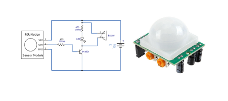
3.1 PIR Sensor Selection and Circuitry
Passive infrared sensors are the most common choice for motion detection in lighting applications. The key parameters for PIR sensor selection include:
- Detection range (typically 5-12 meters)
- Field of view (usually 110-180 degrees)
- Sensitivity adjustment capability
- Output signal type (digital or analog)
The PIR sensor circuit requires careful design of:
- Proper biasing and power supply filtering
- Signal conditioning components
- Sensitivity adjustment potentiometers
- Output interface to the microcontroller
3.2 Microcontroller Selection
The microcontroller serves as the brain of the system, processing sensor inputs and controlling the light output. Important considerations include:
- Low power consumption for battery-operated units
- Sufficient I/O pins for all system functions
- Analog-to-digital conversion capability if using analog sensors
- Appropriate clock speed for response time requirements
- Programming and debugging interfaces
Popular choices include ATtiny series (for simple designs) or ARM Cortex-M0 chips (for more advanced implementations).
3.3 LED Driver Circuit
The lighting module requires an efficient LED driver circuit capable of:
- Delivering constant current to LEDs
- Supporting PWM dimming if variable intensity is desired
- Handling thermal management considerations
- Providing overcurrent and overvoltage protection
For typical motion-activated lights, a buck converter or linear current regulator is often sufficient.
3.4 Power Supply Design
The power supply subsystem must provide:
- Stable voltage to all components
- Sufficient current capacity for peak loads
- Low quiescent current for energy efficiency
- Protection against voltage spikes and reverse polarity
Considerations include:
- Battery vs. mains-powered operation
- Voltage regulation requirements
- Energy harvesting options for solar-powered units
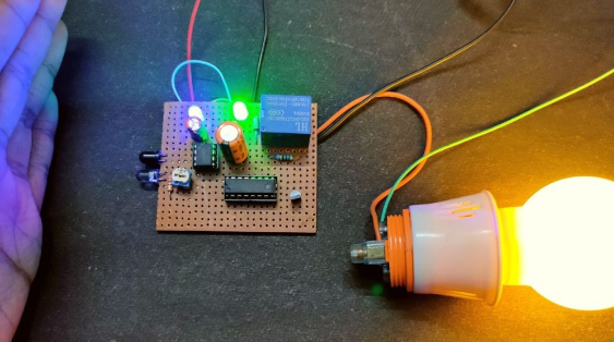
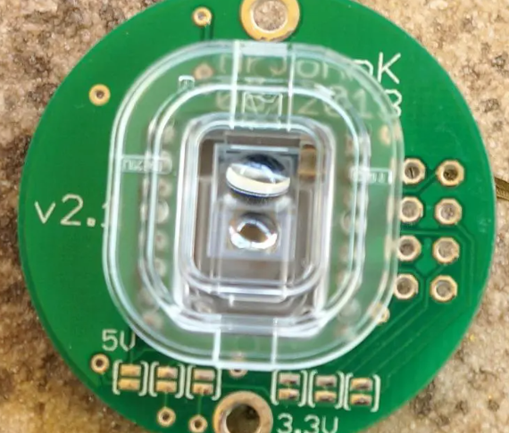
4. PCB Design Implementation
4.1 Schematic Design
The schematic should clearly represent:
- All functional blocks with proper interconnections
- Component values and part numbers
- Power and ground distribution
- Test points for debugging
- ESD protection where needed
4.2 Component Placement
Optimal component placement considers:
- Proximity of related components to minimize trace lengths
- Thermal management of power components
- Mechanical constraints of the enclosure
- Antenna effect minimization for sensitive analog circuits
- Accessibility for manual assembly or rework
4.3 Routing Considerations
PCB routing requires attention to:
- Proper trace widths for current carrying capacity
- Controlled impedance for high-speed signals
- Minimization of noise coupling between analog and digital sections
- Ground plane design for signal integrity
- Thermal relief patterns for hand soldering
4.4 Layer Stackup
For this application, a 2-layer board is typically sufficient:
- Top layer: Signal routing and component placement
- Bottom layer: Ground plane with some power routing
Four-layer boards may be warranted for more complex designs requiring:
- Dedicated power planes
- Better EMI control
- Higher component density
4.5 Design for Manufacturing (DFM)
DFM considerations include:
- Adherence to minimum trace/space rules for the target fabrication process
- Proper pad sizes for components
- Solder mask and silkscreen clearances
- Fiducial marks for automated assembly
- Panelization considerations for mass production
5. Firmware Development
The microcontroller firmware handles:
- Sensor data acquisition and processing
- Motion detection algorithms
- Timing control for light duration
- Optional features like dimming patterns or ambient light adaptation
- Power management for energy efficiency
Key firmware components include:
- Initialization routines for all peripherals
- Interrupt service routines for sensor inputs
- Timing functions for light duration control
- State machines for system operation modes
- Debugging and diagnostic features
6. Testing and Validation
Comprehensive testing should verify:
- Motion detection range and sensitivity
- Light activation and deactivation timing
- Power consumption in all operating modes
- Environmental robustness (temperature, humidity)
- EMI/EMC compliance
- Long-term reliability
Test procedures should include:
- Bench testing with controlled motion sources
- Field testing in intended environments
- Accelerated life testing
- Failure mode analysis
7. Advanced Features and Enhancements
Modern motion-activated lights can incorporate additional features:
- Ambient light sensing to prevent activation during daylight
- Wireless connectivity for remote monitoring/control
- Multi-zone detection with sensor arrays
- Machine learning for improved motion pattern recognition
- Energy harvesting capabilities
- Smart home integration
8. Conclusion
The design of a PCB-based motion-activated lighting system requires careful consideration of multiple technical aspects, from sensor selection to power management. By following proper PCB design practices and selecting appropriate components, designers can create efficient, reliable products that meet the growing demand for intelligent lighting solutions.
Future developments in this field will likely focus on increased integration, improved energy efficiency, and enhanced connectivity options. The continued advancement of PCB technologies and component miniaturization will enable even more sophisticated motion-activated lighting systems in compact, cost-effective form factors.