The Relationship Between Layout and PCB in Electronic Design
Introduction
In the realm of electronic design, the terms “layout” and “PCB” (Printed Circuit Board) are intimately connected, representing two fundamental aspects of bringing electronic circuits from concept to reality. While these terms are sometimes used interchangeably by those outside the field, they actually represent distinct but deeply interrelated stages in the electronic design process. This article explores the nuanced relationship between layout and PCB, examining how they interact, depend on each other, and collectively contribute to successful electronic product development.
Understanding the Basic Concepts
What is a PCB?
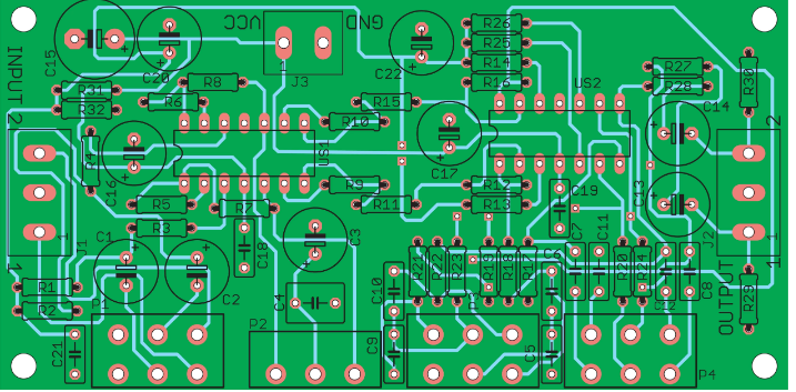
A Printed Circuit Board (PCB) is the physical platform that mechanically supports and electrically connects electronic components using conductive tracks, pads, and other features etched from copper sheets laminated onto a non-conductive substrate. PCBs form the foundation of nearly all modern electronic devices, from simple consumer gadgets to complex aerospace systems.
PCBs can be single-layer (one copper layer), double-layer (two copper layers), or multi-layer (several copper layers separated by insulating material). The complexity of a PCB depends on the circuit it needs to support, with high-density designs requiring sophisticated manufacturing techniques.
What is Layout in Electronic Design?
Layout, in the context of electronic design, refers to the process of arranging components and routing electrical connections on a PCB. It’s the stage where the schematic diagram—an abstract representation of the electrical connections—is transformed into a physical design that can be manufactured.
The layout process involves:
- Component placement
- Routing of electrical connections
- Ensuring proper spacing and clearances
- Managing signal integrity
- Addressing electromagnetic compatibility (EMC) issues
- Considering thermal management
- Planning for manufacturability
The Symbiotic Relationship Between Layout and PCB
From Schematic to Physical Reality
The relationship between layout and PCB is fundamentally about translation—converting an electrical concept into a manufacturable physical object. The schematic represents the ideal electrical connections, while the layout determines how those connections will actually be implemented on the PCB.
A well-executed layout:
- Maintains the electrical characteristics specified in the schematic
- Accounts for real-world physical constraints
- Ensures reliable operation under expected environmental conditions
- Facilitates efficient manufacturing and assembly
Design Constraints and Requirements
The PCB imposes physical constraints that the layout must accommodate:
- Board Dimensions: The layout must fit within the specified board outline.
- Layer Stackup: The number and arrangement of copper layers affect routing options.
- Material Properties: The substrate material impacts signal speed and thermal characteristics.
- Manufacturing Capabilities: Minimum trace widths, spacing, and hole sizes must be respected.
Conversely, the layout requirements influence PCB specifications:
- Component Density: High-density layouts may require more layers or advanced manufacturing.
- Signal Speed: High-speed signals may demand specific layer stackups or materials.
- Power Requirements: High-current paths may need thicker copper or thermal relief.
- Environmental Factors: Harsh environments may dictate material choices or conformal coatings.
Key Aspects of the Layout-PCB Relationship
1. Component Placement and Board Organization
The layout process begins with component placement, which significantly impacts the PCB’s functionality, manufacturability, and reliability. Good placement considers:
- Functional Grouping: Related components placed together to minimize connection lengths
- Signal Flow: Logical arrangement following the schematic’s signal paths
- Thermal Considerations: Heat-generating components spaced appropriately
- Mechanical Constraints: Accounting for enclosures, connectors, and mounting points
- Manufacturing Requirements: Placement for automated assembly processes
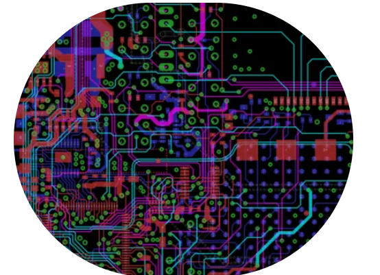
2. Routing and Layer Utilization
The layout’s routing strategy depends on the PCB’s layer stackup:
- Single-layer Boards: Require creative routing as all connections must exist on one plane
- Double-layer Boards: Allow more routing flexibility with top and bottom layers
- Multi-layer Boards: Enable complex routing with dedicated layers for signals, power, and ground
Advanced layouts often employ:
- High-Density Interconnect (HDI): Microvias and fine-pitch components for compact designs
- Controlled Impedance Routing: Precise trace dimensions for high-speed signals
- Differential Pairs: Carefully matched routing for noise immunity
3. Signal Integrity and PCB Characteristics
The layout must account for how PCB properties affect electrical performance:
- Transmission Line Effects: At high frequencies, traces behave as transmission lines
- Crosstalk: Adjacent traces can interfere with each other
- Return Paths: Continuous reference planes are crucial for signal quality
- Power Distribution: Proper decoupling and power plane design
4. Thermal Management
The layout directly affects how heat is dissipated on the PCB:
- Component Spacing: Allows for adequate airflow
- Thermal Relief: Connections that balance electrical and thermal needs
- Copper Pour: Large copper areas that act as heat spreaders
- Via Arrays: Help transfer heat between layers
5. Manufacturability and Assembly
The layout must consider how the PCB will be manufactured and assembled:
- Design for Manufacturing (DFM): Adhering to fabrication capabilities
- Design for Assembly (DFA): Facilitating component placement and soldering
- Testability: Including test points for quality control
- Panelization: Efficient use of manufacturing panels
The Layout-to-PCB Workflow
- Schematic Capture: Creating the circuit diagram
- Component Selection: Choosing parts with known footprints
- Board Outline Definition: Establishing physical dimensions
- Layer Stackup Design: Determining PCB material and layer structure
- Placement: Arranging components on the board
- Routing: Connecting components according to the schematic
- Design Rule Checking (DRC): Verifying manufacturability
- Output Generation: Creating files for fabrication and assembly
Advanced Considerations in the Layout-PCB Relationship
High-Speed Design
Modern high-speed circuits require careful attention to:
- Impedance Control: Matching trace impedance to system requirements
- Length Matching: Ensuring critical signals arrive simultaneously
- EMI Reduction: Minimizing electromagnetic interference
- Power Integrity: Maintaining stable voltage distribution
RF and Microwave Layouts
Radio frequency designs demand:
- Transmission Line Structures: Microstrip or stripline configurations
- Grounding Strategies: Preventing ground loops and ensuring stable references
- Component Parasitics: Accounting for unintended inductance and capacitance
Flexible and Rigid-Flex PCBs
These specialized boards require layouts that consider:
- Bend Areas: Routing and component placement in flexible sections
- Transition Zones: Connections between rigid and flexible areas
- Dynamic Flexing: Ensuring reliability during movement
Tools and Technologies Supporting the Layout-PCB Relationship
Modern electronic design automation (EDA) tools facilitate the layout-to-PCB process:
- Schematic Capture Tools: Create the electrical diagram
- PCB Layout Software: Translate schematics to physical designs
- 3D Modeling: Visualize components and enclosures
- Signal Integrity Analysis: Predict electrical performance
- Thermal Simulation: Analyze heat distribution
- Manufacturing Output Generators: Create fabrication files
Common Challenges in the Layout-PCB Relationship
- Design Iterations: Layout limitations may require schematic changes
- Component Availability: Footprint changes may affect layout
- Cost Constraints: Balancing performance with manufacturing costs
- Time-to-Market Pressures: Accelerating the design process
- Miniaturization Demands: Packing more functionality into smaller spaces
Best Practices for Harmonizing Layout and PCB Requirements
- Early Collaboration: Involve all stakeholders from the beginning
- Design Reviews: Regular checkpoints to catch issues early
- Prototyping: Test critical aspects before full production
- Documentation: Maintain clear records of design decisions
- Continuous Learning: Stay updated on materials and technologies
Future Trends Affecting the Layout-PCB Relationship
- Embedded Components: Passive components within the PCB layers
- Advanced Materials: Higher frequency and thermal performance
- Additive Manufacturing: 3D printing of circuit structures
- AI-Assisted Design: Automated layout optimization
- Sustainable Practices: Eco-friendly materials and processes
Conclusion
The relationship between layout and PCB represents one of the most critical interfaces in electronic design—where abstract electrical concepts meet physical reality. A successful design harmonizes the schematic’s electrical requirements with the PCB’s physical constraints through thoughtful layout. As electronic devices continue to evolve, becoming more complex, miniaturized, and performance-demanding, the interplay between layout and PCB will grow even more significant. Understanding this relationship is essential for anyone involved in electronic product development, from designers and engineers to project managers and manufacturing specialists. By mastering the delicate balance between layout considerations and PCB realities, designers can create robust, reliable, and manufacturable electronic products that meet the ever-increasing demands of modern technology.