Do you know the design and processing of PCB gold finger?
1.Definition of gold finger
(Gold Finger or Edge Connector) Insert one end of the PCB into the connector slot, use the connector pin as the outlet for the PCB to connect to the outside, make the pad or copper contact with the corresponding position of the pin to achieve the purpose of conduction, and immerse gold or plate nickel gold on the pad or copper of the PCB. Because it is in the shape of a finger, it is called a gold finger.
2.Surface treatment of gold finger PCB
1.Electroplating nickel gold:
The thickness can reach 3-50u”. Due to its superior conductivity, oxidation resistance and wear resistance, it is widely used in gold finger PCBs that need to be frequently plugged in or PCBs that need to be frequently mechanically rubbed. However, because the cost of gold plating is extremely high, it is only used for local gold plating such as gold fingers. Jieduobang PCB calls it: selective electroplating gold process. The color of electroplating gold process is silvery white, not as yellow as immersion gold. The disadvantage is that the solderability is slightly poor.
2.Immersion gold:
The thickness is usually 1u”, and the maximum can reach 3u”. Due to its superior conductivity, flatness and solderability, it is widely used in high-precision PCB boards with key positions, IC binding, BGA and other designs. For gold finger PCBs with low wear resistance requirements, the whole board immersion gold process can also be selected. The cost of the immersion gold process is much lower than that of the electroplating gold process. The color of the immersion gold process is golden yellow.
3.Matters needing attention in gold finger design
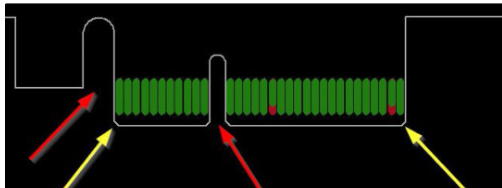
When you see the shape and package similar to the figure below when designing PCB, the first reaction is that there are gold fingers on the board. A relatively simple way to judge the gold fingers: There are PIN devices on the TOP and BOTTOM surfaces of the device; there will be a fool-proof U-shaped groove as shown in the figure below.
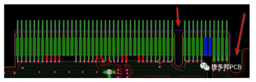
When there are gold fingers on the board, the details of the gold fingers need to be processed.
Detailed processing of gold fingers in PCB:
1) For PCB boards that need to be plugged and unplugged frequently, in order to increase the wear resistance of the gold fingers, the gold fingers usually need to be electroplated with hard gold.
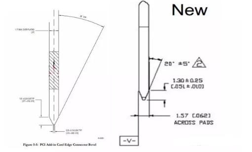
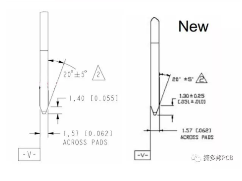
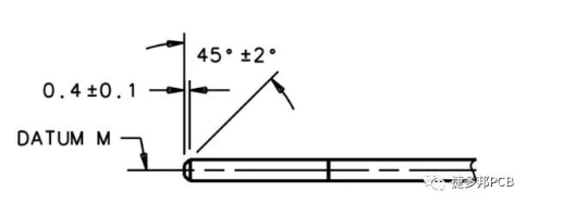
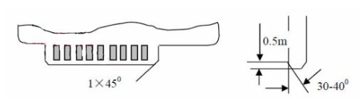
2) Gold fingers need to be chamfered, usually 45°, other angles such as 20°, 30°, etc. If there is no chamfer in the design, there is a problem; as shown in the figure below, the arrow indicates a 45° chamfer:
3) Gold fingers need to be processed with a whole piece of solder mask opening, and PIN does not need to open a steel mesh;
4) The minimum distance between the tin and silver pads and the top of the finger is 14mil; it is recommended that the pads be more than 1mm away from the finger during design, including the via pads;
5) Do not lay copper on the surface of the gold finger;
The following figure is a design of a gold finger for reference:
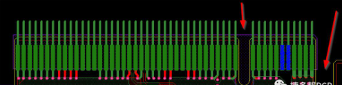
6) All layers of the inner layer of the gold finger need to be copper-cut, usually with a width of 3mm; half-finger copper cutting and whole-finger copper cutting can be done. In PCIE design, it is also specified that all copper in the gold finger area should be cut off;
The impedance of the gold finger will be relatively low, and copper cutting (hollowing out under the finger) can reduce the impedance difference between the gold finger and the impedance line, and it is also good for ESD;
Recommendation: Full copper cutting under the gold finger pad.
4.PCB gold finger processing of JDB
1.The thickness of the board that can be beveled can be processed with a thickness of 1.2-2.4m. The bevel cannot be processed if it is not within this thickness range.
2.The depth and angle of the bevel are generally between 20-45 degrees by default. There must be enough bevel spacing between the gold finger and the board edge. According to the board thickness or design requirements of different gold finger PCBs, we recommend that the distance between the gold finger and the board edge is 0.6-1.5mm during design to avoid damaging the gold finger during beveling. If the distance between the gold finger and the board edge is less than 0.6mm, there is a risk of damaging the gold finger if beveling is required. The following are several common bevel angle and depth diagrams for your reference.