PCB Design, Manufacturing, and Processing: A Comprehensive Guide
1. Introduction
Printed Circuit Boards (PCBs) are the backbone of modern electronics, providing mechanical support and electrical connections for electronic components. From consumer electronics to aerospace applications, PCBs are essential in ensuring the functionality and reliability of electronic devices. This article explores the entire PCB lifecycle, including design, manufacturing, and processing, while highlighting key considerations for engineers and manufacturers.
2. PCB Design
2.1 Schematic Design
The PCB design process begins with a schematic diagram, which represents the electrical connections between components. Engineers use Electronic Design Automation (EDA) software such as Altium Designer, KiCad, or Cadence OrCAD to create schematics. Key considerations include:
- Component selection (resistors, capacitors, ICs, etc.)
- Power requirements (voltage, current, and grounding)
- Signal integrity (minimizing noise and interference)
2.2 PCB Layout Design
Once the schematic is finalized, the next step is PCB layout design, which involves:
- Component placement (optimizing space and minimizing signal interference)
- Routing (copper traces for electrical connections)
- Layer stack-up (single-layer, double-layer, or multi-layer PCBs)
- Design Rule Check (DRC) (ensuring manufacturability and avoiding errors)
2.3 Key Design Considerations
- Signal Integrity: High-speed signals require controlled impedance routing.
- Thermal Management: Proper heat dissipation through thermal vias and copper pours.
- EMI/EMC Compliance: Shielding and grounding to reduce electromagnetic interference.
- Manufacturability (DFM): Avoiding overly complex designs that increase production costs.
3. PCB Manufacturing Process
After the design is finalized, the PCB moves to the manufacturing phase. The process involves several critical steps:
3.1 Material Selection
- Substrate (FR-4, Rogers, Polyimide): FR-4 is the most common due to its cost-effectiveness and durability.
- Copper Cladding: Typically 1 oz/ft² (35 µm) or 2 oz/ft² (70 µm) for higher current applications.
3.2 PCB Fabrication Steps
- Printing the Design: A photomask is created from the PCB layout.
- Copper Etching: Unwanted copper is removed using chemical etching.
- Drilling: Holes for through-hole components and vias are drilled.
- Plating: Copper is electroplated to strengthen connections.
- Solder Mask Application: A protective layer (usually green) is applied to prevent short circuits.
- Silkscreen Printing: Component labels and logos are printed.
- Surface Finish: Options include HASL (Hot Air Solder Leveling), ENIG (Electroless Nickel Immersion Gold), or OSP (Organic Solderability Preservative).
3.3 Multi-Layer PCB Fabrication
For complex designs, multi-layer PCBs are used. The layers are laminated together under high pressure and temperature.
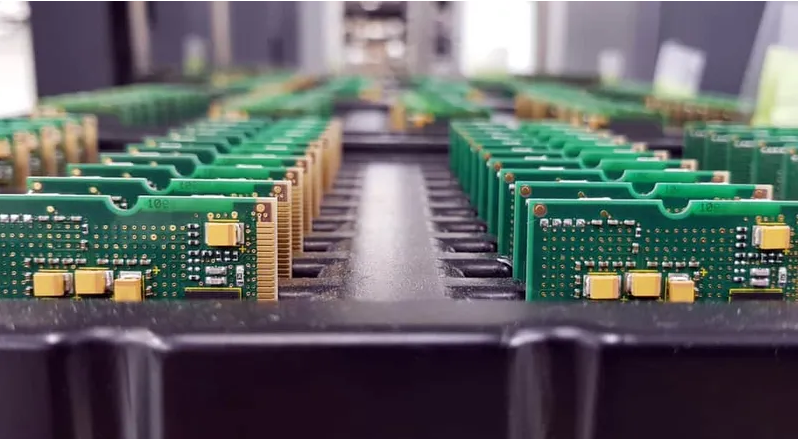
4. PCB Assembly (PCBA)
After fabrication, components are mounted on the PCB through:
4.1 Surface Mount Technology (SMT)
- Pick-and-Place Machines automatically place components.
- Reflow Soldering melts solder paste to create connections.
4.2 Through-Hole Technology (THT)
- Components with leads are inserted into drilled holes.
- Wave Soldering is used for bulk soldering.
4.3 Inspection & Testing
- Automated Optical Inspection (AOI) checks for defects.
- In-Circuit Testing (ICT) verifies electrical performance.
- Functional Testing ensures the PCB operates as intended.
5. Advanced PCB Technologies
5.1 High-Density Interconnect (HDI) PCBs
- Uses microvias and finer traces for compact designs (e.g., smartphones).
5.2 Flexible & Rigid-Flex PCBs
- Made from polyimide for bendable applications (wearables, medical devices).
5.3 High-Frequency PCBs
- Designed for RF/microwave applications (5G, radar systems).
6. Challenges in PCB Manufacturing
- Miniaturization: Smaller components require precision manufacturing.
- Thermal Stress: Warping due to heat during soldering.
- Signal Loss: High-frequency designs need careful impedance control.
7. Future Trends in PCB Technology
- 3D Printed PCBs: Faster prototyping with additive manufacturing.
- Embedded Components: Passive components integrated into the PCB substrate.
- AI in PCB Design: Machine learning optimizes layouts for performance and cost.
8. Conclusion
PCB design, manufacturing, and assembly are complex processes requiring expertise in electronics, materials science, and mechanical engineering. As technology advances, PCBs will continue to evolve, enabling smaller, faster, and more efficient electronic devices. Engineers must stay updated with the latest trends to ensure high-quality PCB production.
By understanding the entire PCB lifecycle—from design to assembly—manufacturers can optimize performance, reduce costs, and deliver reliable products for the ever-growing electronics industry.