5 Common Mistakes That Lead to PCB Failure
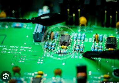
An integral part of most electronic and electrical devices nowadays, the Printed Circuit Board (PCB) essentially consists of copper traces of different components connected together to create a complex maze of circuits. The importance of PCBs can be directly measured by the fact that any error in its design or assembly will affect the performance and output of the final product. Whether you are manufacturing PCBs for a small electrical company or a global technology giant, complications and challenges arise during the PCB assembly process that severely affect the quality of the final product. Smooth collaboration is a must as far as PCB assembly is concerned, and all stakeholders including designers, engineers, manufacturers, and fabricators need to work together to ensure that the assembly process goes smoothly and is error-free. Defective PCB assemblies can ultimately cost an organization dearly in terms of reputational loss and returned deliveries.
The possibility of errors during PCB assembly exists at any process step, it could be a result of a flaw in the technical design itself, or it could be a product of an operational error. While there could be any number or reasons for errors during the PCB assembly process, here are 5 of the most common errors that lead to PCB failure.
Flex Cracking
The term flex cracking is used when excessive stress on a ceramic chip capacitor causes the PCB to bend excessively while passing through it. Ceramic chip capacitors are designed to withstand specific loads, and when the load generated by the PCB exceeds its maximum capacity, it will stress the ceramic chip capacitor, causing the PCB to bend. It is very important to use the same or similar load-rated ceramic chip capacitors during the design phase to ensure that the capacitors will not be stressed and cause the PCB to bend or crack, ultimately leading to PCB performance failure.
No Obvious Polarity
Assembling PCBs requires many different components, such as batteries and diodes, which are characterized by polarity. Marking the polarity of each individual component is very important to make it easy for assembly engineers to distinguish between anodes and cathodes. If the polarity is not clearly marked or is marked incorrectly, there is a high chance that the wrong polarity will be connected to the wrong terminal during the PCB assembly process. Short circuits in PCBs are often caused by incorrect connections between polarity and terminals, and can even cause the circuit to explode, or at least cause some components on the PCB to be completely destroyed.
Insufficient Copper to Edge Clearance
Coppers high conductive properties make it an ideal metal in electrical and electronic PCBs. However, as a metal, copper is also very susceptible to corrosion, which will occur if the copper layer is exposed to the environment. This is why the copper used in PCB assembly is often coated with other materials, such as plastic, to prevent corrosion. But sometimes during the process of trimming the printed circuit board, the copper coating is also trimmed, causing the layers underneath to be exposed to the environment, increasing the likelihood of corrosion and PCB failure. This mistake can be easily avoided by ensuring that the space between the edge of the board and the copper edge (also known as the internal clearance or copper-to-edge clearance) follows specific quality standards.
Plating Clearance or Voids
An important part of the PCB assembly process is the electroplating deposition process. This process is used to drill holes in the board through which electricity can be carried from one end of the board to the other. Once the holes are drilled, a thin layer of electroless copper is added to the board and along the walls of the holes, which serves as a foundation for subsequent layers used to etch the printed circuit board. Errors in the deposition process can result in copper-plated holes that prevent current from flowing through the holes, causing the entire PCB to fail.
Component Misalignment
Each component on a printed circuit board has a specific landing point. Sometimes, during the soldering process, components are displaced from their target location by attaching themselves to the molten solder. Misaligned components can disrupt the normal flow of electricity through the board, causing the entire PCB to fail. It is only in cases where the entire assembly is missed during the assembly process that the system fails.
Conclusion
PCB assembly requires skills and expertise, but even then, there is scope unless you employ adequate quality control measures at every stage of the PCB assembly process to ensure that a small error in assembly does not cause the entire product to fail.