Impact of Different pcb and component deploy for thermal behavior
1.Introduction
In the previous chapter the effects of different PCB and device configurations on thermal behavior were considered. By analyzing and comparing a number of scenarios, a number of conclusions can be drawn about the best way to provide heat sink cooling for LFPAK MOSFETs.
All of the PCB configurations considered in Chapter 4 had one thing in common – they were all in free air at an ambient temperature of 20°C. No enclosure was included in the scenarios. However, in most practical applications we will probably not have a PCB without an enclosure. To protect the PCB from environmental factors, plus perhaps for electromagnetic compatibility (EMC) considerations, it is almost certain that the PCB will be mounted in some form of enclosure. Inevitably, the enclosure will interfere with the free flow of air around the PCB and therefore also have an impact on the thermal performance of the system.
In this chapter we will take a closer look at how the construction and configuration of an enclosure can affect the operating temperature inside a power MOSFET device. Factors that will be examined include:
- Enclosure material and enclosure finish
- Internal spacing between upper and lower enclosures and surrounding PCB
- Bottom cooling of the PCB (i.e., the bottom surface of the PCB is in contact with the inner surface of the enclosure)
- Top cooling of the MOSFET device (the top of the device is in contact with the inner surface of the enclosure)
- The role of the package inside the package, i.e., the air gap around the PCB is partially or completely filled with potting compound
- “Modules” near the bulkhead
To rationalize the number of possible variables, we will consider only one PCB configuration, taken from Chapter 4. Appendix plus
The PCB will be referred to as a “module” henceforth.
As in Chapter 4, the thermal design experiments in this chapter were performed using thermal simulation software. These simulations used MOSFET models that have been validated against empirical data and are known to accurately simulate the thermal behavior of real devices.
The thermal simulation software used to perform the design experiment analysis was the Mentor graphic (Flomerics) “FloTHERM” software package.
2.Module Model
(1) PCB Characteristics
To minimize the number of possible variables, we will consider only one PCB configuration, taken from Section 4.5.4. The PCB is shown in Figure 1.
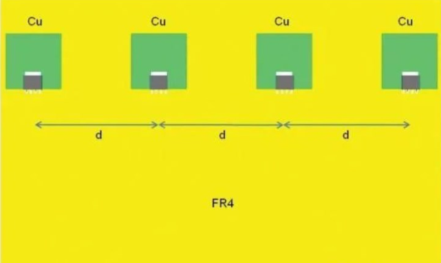
Figure 1: PCB Model
The main characteristics of the PCB are:
- Overall PCB size 80mmx120mm, thickness 1.6mm standard
- FR4 PCB material
- 1oz/35µm copper layer thickness
- Top copper – 15mmx15mm area per device, connected to the device Tab (as shown) Bottom copper – 15mmx15mm area per device, connected to the top copper through thermal vias
- Internal layers – 50% area coverage on average
- Thermal vias – Under each device, a pattern of 5×4 thermal vias with 0.8mm inner diameter Device spacing d=25mm
- Power consumption per device is 0.5W
Chapter 4 pointed out that the location of individual Mosfets has little effect on their operating temperature, with an effect of only about ±1℃.
(2)Enclosure Characteristics
Throughout this chapter, there will be a number of different enclosure characteristics. However, some general characteristics will always remain the same:
- The enclosure is completely sealed with no holes or seams.
- The wall thickness of the enclosure is 2mm, regardless of the enclosure material.
- The enclosure is capable of losing thermal energy to the outside environment through convection, conduction, and radiation mechanisms.
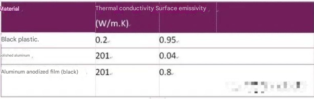
Several different enclosure materials may be considered in this design guide. In order to keep the number of variables to a manageable level while also providing a useful realistic analysis of typical materials, we will limit our focus to the following three variables, as shown in Table 1. Table 1 provides an overview of enclosure materials and their properties
Surface radiation applies to both the inside and outside surfaces of the enclosure.
Figure 2 shows an example module. Note that the top and one side of the enclosure are transparent so that the PCB can be seen.
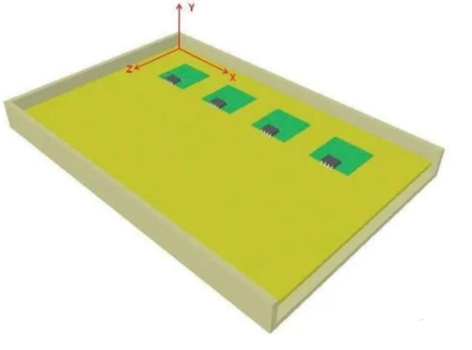
Figure 2 shows a module
(3)Axis Naming Convention
In this chapter, we will consider the effects of moving or resizing an object in three spatial directions. Therefore, we need a convention for referencing these directions, as shown by the arrows in Figure 2.
For example, when we add a gap between the PCB and the housing on the short side of the PCB (x-direction), this will be called an “x-gap”. Similarly, the gap above and below the PCB will be called a “y-gap”, and so on.
(4) Surrounding Environment
The module is located in an environment with the following characteristics:
- The module is surrounded by free air at an ambient temperature of 20°C
- There is no applied airflow, although the module is able to generate airflow through natural convection processes on the external surfaces
- The environment is free to exchange thermal energy with the module through convection, conduction, and radiation processes
(5)Potential Thermal Paths
There are many possible paths by which heat can travel through a PCB. These paths utilize the three heat transfer mechanisms of conduction, convection, and radiation, as shown in Figure 3.
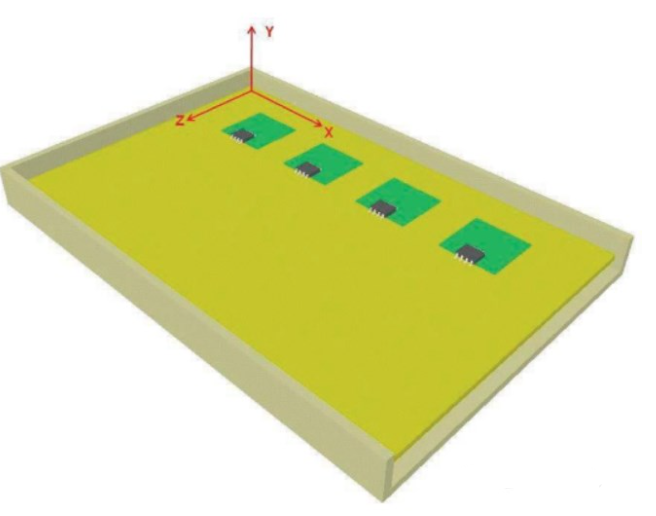
Figure 3: Potential Thermal Paths