4 Types of PCB Solder Masks
Solder mask, also known as solder block mask, is a thin layer of polymer used on PCB boards to prevent solder joints from forming bridges. Solder mask also prevents oxidation and is applied to the copper traces on the PCB board.
That’s a quick answer, then we’ll delve into some details because not all solder masks are the same!
What are PCB solder mask types? PCB solder mask acts as a protective coating on copper traces, preventing rust and stopping solder from forming bridges that cause short circuits. There are 4 main PCB solder mask types – epoxy liquid, liquid photoimageable, dry film photoimageable, top and bottom mask.
But which PCB solder mask type should you use? That’s right, there are different types for different uses… let’s take a look.
4 Types of Solder Masks
Solder masks vary in make and material. How and which solder mask to use depends on the application.
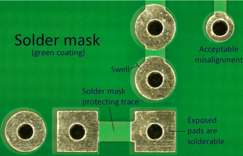
Top and Bottom Side Masks
Top and Bottom Solder Masks Electronics engineers commonly use it to identify openings in the green solder mask layer. This layer is pre-added via epoxy or film technology. The component pins are then soldered on the board using the openings registered using the mask.
The conductive trace pattern on the top of the board is called top traces. Similar to the top side mask, the bottom side mask is used on the reverse side of the board.
Epoxy Liquid Solder Mask
Epoxy is the cheapest alternative to solder mask. Epoxy is a polymer that is screen printed on the PCB. Screen printing is a printing method that employs a fabric mesh to support the ink blocking pattern. The mesh allows for the identification of open areas for ink transfer. In the final step of the process, heat curing is used.
Liquid Photoimageable Solder Mask
Liquid photoimageable mask, also known as LPI, is actually a mixture of two different liquids. The liquid components are mixed before application to ensure a longer shelf life. It is also one of the more economical products among the four different PCB solder mask types.
LPI can be used for screen printing, curtain coating or spray application. The mask is a mixture of different solvents and polymers. As a result, a thin coating can be extracted, which adheres to the surface of the target area. This mask is used for the original purpose of solder mask, but the PCB does not require any final plating coating that is commonly available today.
Contrary to the old epoxy inks, LPI is sensitive to UV light. The panel needs to be covered with a mask. After a short “curing cycle”, the board is exposed to UV light using a photolithography or UV laser.
Before applying the mask, the panel needs to be cleaned and free of signs of oxidation. This is done with the help of special chemical solutions. It can also be done using an aluminum oxide solution or by scrubbing the panel with a suspended pumice stone.
One of the most common methods of exposing the panel surface to UV light is to use a contact printer and a film tool. The top and bottom sheets of the film are printed using emulsion to block the areas that will be soldered. The production panel and the film are fixed in their position using a tool on the printer. Subsequently, the panel is simultaneously exposed to a UV light source.
Another technique uses direct laser imaging. But in this technique, no film or tool is needed, as the laser is controlled using fiducial marks on the panel’s copper stencil.
LPI masks can be found in a variety of colors including green (matte or semi-gloss), white, blue, red, yellow, black, and many more. The LED industry and laser applications in the electronics industry have encouraged manufacturers and designers to develop more robust white and black materials.
Dry Film Photoimageable Solder Mask
With dry film photoimageable solder masks, vacuum lamination is used. The dry film is then exposed and developed. After the film is developed, the openings are positioned to create a pattern. Following this, components are soldered to the copper pads. The copper is then laminated to the board using an electrochemical process.
The copper is layered inside the holes as well as within the trace areas. Tin is ultimately used to help protect the copper circuitry. In the final step, the film is removed and the etch marks are exposed. This process also uses heat curing.
Dry film solder mask is often used for high-density wiring boards. As a result, it does not flood into the through-holes. These are some of the positive factors for using dry film solder mask.
Deciding which solder mask to use depends on a variety of factors – including the physical size of the PCB, the end application it will be used in, the holes, the components to be used, the conductors, the surface layout, and more.
Most modern PCB designs get a photoimageable solder mask. So, it is either LPI or dry film solder mask. The surface layout of the board will help you determine the final choice. If the surface topography is uneven, then LPI mask is preferred. If dry film is used on uneven topography, there is a possibility of gas being trapped in the space formed between the film and the surface. Therefore, LPI is more suitable here.
However, there are also disadvantages to using LPI. It is not uniform across the board. You can also get different finishes on the mask layer, each with its own application. For example, a matte finish will reduce solder balls in case solder reflow is used.
Build solder mask into your design
Building solder mask into your design is integral to ensure that the mask application is at an optimal level. When designing the board, the solder mask should have its own layer in the Gerber file. Generally, it is recommended to use a 2mm border around the features in case the mask is not perfectly centered. You should also leave at least 8mm between copper pads to ensure that solder bridges do not form.
Solder Mask Thickness
The thickness of the solder mask will depend on the thickness of the copper traces on your board. Typically, a 0.5mm solder mask is preferred to mask the traces. If you are using a liquid mask, then you must have different thicknesses on different features. Empty laminate areas may have a thickness of 0.8-1.2mm, while areas with complex features (like knees) will have thin extensions (around 0.3mm).
Conclusion
In conclusion, solder mask design has a serious impact on the functionality of your application. It plays a vital role in preventing rust and solder bridges (which can cause short circuits). Therefore, your decision needs to consider the different factors mentioned in this article. Hopefully, this article has helped you understand PCB solder mask types better. If you have any questions, or just need to get in touch with us, we are always happy to help you.