PCB sub-board stress test method and steps
The main purpose of PCB mechanical stress test is to evaluate the performance and stability of PCB boards under different environmental conditions and load conditions. Through stress testing, potential design defects, material defects and manufacturing process problems can be found, so that corresponding measures can be taken to improve them, so as to improve the reliability and service life of PCB boards.
When PCBA undergoes SMT, DIP, assembly and reliability testing, excessive mechanical stress will cause self-failure. Common concentrated modes of failure due to mechanical stress include: solder ball cracking, circuit damage, pad lift, substrate cracking, capacitor Y-type cracking and 45° type cracking.
The following details the method and steps of PCB sub-board stress test
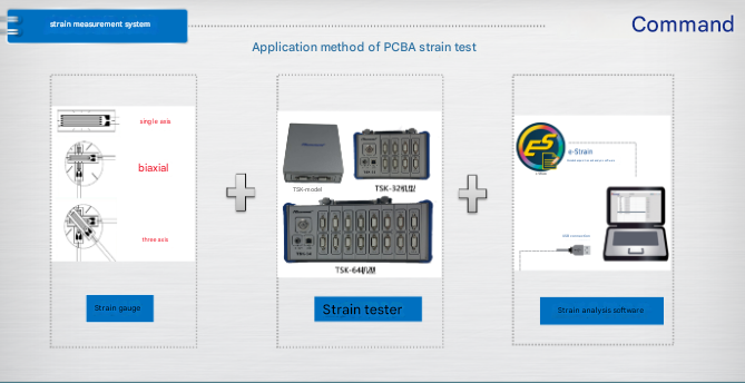
I.Selection of stress tester and strain gauge
Stress tester: Select the multi-channel TSK-32 model or DL-1000 model.
Strain gauge: Select the triaxial strain gauge TSK-1E-120-3A-11L50W05MS.
Test software: A computer with e-strain software installed.
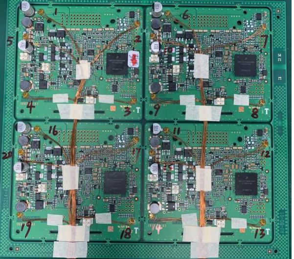
II.Mount the strain gauge in the designated place
(1)BGA devices
BGAs larger than 2727mm are required, including but not limited to FCBGA and CBGA. If there is no BGA larger than 2727mm on the board, the largest BGA on the board or the BGA with concentrated stress is preferred for testing.
(2)Stress sensitive devices
Based on the identification of stress risk points distributed on the board, the following stress sensitive devices are selected for evaluation:
A. Ceramic capacitors and ordinary capacitors (excluding soft terminal capacitors) with 0402 and above packages, and ceramic capacitors tested in ICT, BST and other processes are 1206 and above packages.
B. Stress-prone components such as chip resistors, ceramic crystal oscillators, inductors, magnetic beads, PLO modules, gas discharge tubes, and fuse kits.
III. Connect the instrument
Connect the lead of the strain gauge to the test instrument of the test system, adjust the sampling frequency, filter value, effective range of values, number of channels, configure the main channel data storage directory and other parameters, and run the test program to check whether each channel is connected.
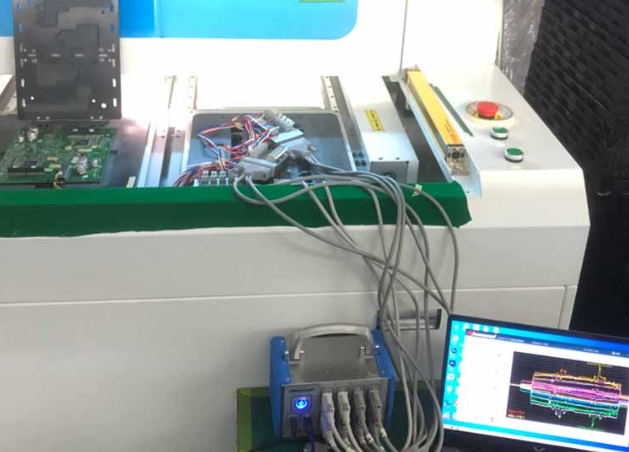
IV. Data measurement
Place the circuit board on the board separation workbench to be measured, adjust the filter value to eliminate external electrical signal interference–click clear–click start, collect data, and then perform the circuit board separation action (screwing, board separation, ICT, etc.), after the action is completed, click stop collection.
V. Issue a report
Import the collected data into the software, fill in the thickness and strain rate range of the board, select the report format, and click Generate Report to generate a stress test report (according to IPC/JEDEC standards, one-click automatic report generation).
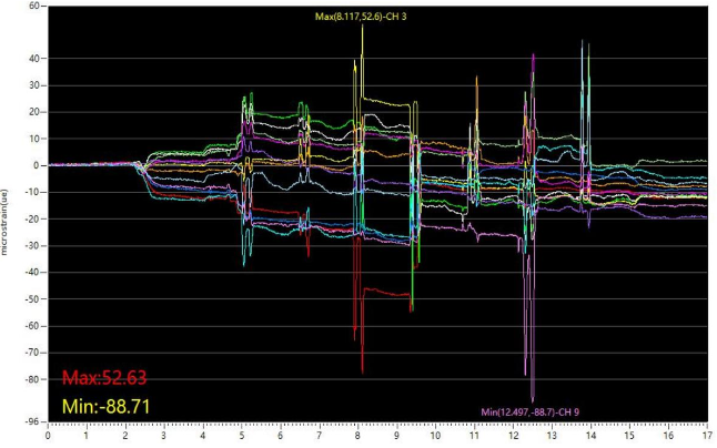
IPC/JEDEC-9704A is a standard document for mechanical strain test operation guidelines for PCBA printed circuit boards. Regarding strain test standards, most customers in the industry currently refer to ±500ue.
IPC/JEDEC-9704A CN Printed Circuit Board Strain Test Guidelines mainly introduces the PCBA strain test guidelines during the printed circuit board manufacturing process. These manufacturing processes include assembly, testing, system integration, and other operations that may cause printed circuit board bending.