How to Make Tradeoffs in PCB Power Design
When designing a complex board, you must make certain design tradeoffs. These tradeoffs influence the design of the PCB’s power distribution network.
When capacitors are mounted on a PCB, they create an additional loop inductance, which is dependent on the capacitor’s placement. The value of this loop inductance is design-dependent. This loop inductance is determined by the trace width and length from the capacitor to the via, the trace length (i.e., the length of the trace connecting the capacitor to the power/ground plane), the distance between the vias, the via diameter, the capacitor’s pad, and other factors. Figure 1 shows various capacitor placement patterns.
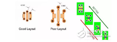
Figure 1: Optimal and Worst Capacitor Layouts
Key Design Tips for Reducing Capacitor Loop Inductance:
■ Place the vias as close to the capacitor as possible. Reduce the spacing between power/ground vias. If possible, use multiple pairs of power/ground vias in parallel. For example, place vias with opposite current polarity as close together as possible, and vias with the same current polarity as far apart as possible.
■ Use short, wide traces to connect vias and capacitor pins.
■ Place capacitors on the PCB surface (top and bottom layers) as close as possible to their corresponding power/ground planes. This minimizes the distance between vias. Use a thin dielectric between the power/ground planes.
Next are three different design scenarios for capacitor mounting and propagation inductance. Figure 2 shows how each design scenario contributes to loop inductance.
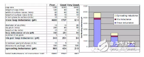
Figure 2 Design Scenarios
Scenario 1 – Poor Design
■ The designer does not pay attention to the power distribution network (PDN) design.
■ The via spacing is not optimized.
■ The distance between the power and ground planes is not optimized.
■ The trace distance between the vias and the capacitor pins is long.
Regarding the overall loop inductance, the primary contributor is the trace length, as the trace length in the poor design is five times longer than in the good and very good designs compared to the other two scenarios. The distance from the bottom layer where the capacitor is mounted to the nearest plane is also a major factor in the loop inductance. Because this is an unoptimized design (10 mil), the trace significantly contributes to the overall loop inductance. Similarly, because the designer used 10 mils of dielectric material between the power and ground planes, the secondary contribution to the loop inductance comes from propagation inductance. The effect of unoptimized via spacing is less pronounced than with smaller via lengths. The impact of vias becomes even greater with longer vias.
Case 2 – Good Design
■ The designer focused on the design of some power distribution networks (PDNs).
■ The via spacing was improved. The via length remained the same.
■ The distance between the power and ground planes was improved.
■ The trace distance between the vias and the capacitor pins was optimized.
The trace loop inductance remains the primary contributor to the overall loop inductance. However, the trace loop inductance in the good design is approximately 2.7 times smaller than that in the poor design. Because the designer reduced the dielectric thickness from 10 mils to 5 mils, the propagation inductance was halved. The impact of the vias was slightly reduced by reducing the via spacing.
Case 3 – Excellent Design
■ The designer paid close attention to the PDN design.
■ The via spacing and length were improved.
■ The distance between the power supply and ground pins was also fully optimized.
■ The trace distance between the via and the capacitor pin was optimized.
The trace inductance of the excellent design is approximately 7.65 times lower than that of the poor design. This is achieved by reducing the trace length and reducing the thickness of the PCB layer from the bottom surface where the capacitor is mounted to the nearest plane. Because the designer optimized the dielectric thickness between the power supply and ground pins, the propagation inductance is significantly reduced. The via loop inductance is also significantly improved due to the significant reduction in the via spacing and length. Compared to the poor design, the total loop inductance of the excellent design is reduced by reducing one of the seven key factors.
Additional via loop inductance introduced by the capacitor on the PCB lowers the capacitor’s resonant frequency. This factor must be taken into account when designing your power distribution network (PDN). When designing at high frequencies, reducing loop inductance is the only visible way to lower impedance.
For a given power supply, the PDN tool reports show that the PCB cutoff frequency is higher for the best design compared to the worst. This may be counterintuitive, as decoupling at higher cutoff frequencies requires more capacitors than decoupling at lower cutoff frequencies.
For the best design, a higher cutoff frequency means decoupling at higher frequencies. Capacitors placed on the PCB provide decoupling for noise up to a higher frequency.
For the worst design, decoupling is impossible above the lower cutoff frequency. Any additional capacitance—that is, adding decoupling capacitors above the cutoff frequency—only increases BOM cost without affecting decoupling effectiveness. Compared to the best design, the power distribution network design of the worst design is more susceptible to noise at a specific frequency.
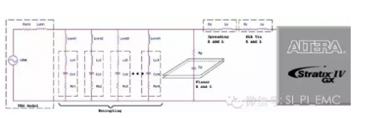
As another example, consider a 20-layer PCB with a total thickness of 115 mils. The power plane is on layer 3. The thickness from layer 1 (where the FPGA is located) to layer 3 is 12 mils. The thickness from the bottom layer to the third layer is 103 mils. The power and ground layers are separated by a 3-mil dielectric. The BGA via inductance for this trace is 5 nH (for this power trace, there are five pairs of vias). To accommodate the dense layout and routing area on the first layer, the associated decoupling capacitors are all mounted on the bottom layer. This trade-off results in high capacitor mounting inductance due to the long vias involved. After full optimization, the mounting inductance of a 0402 package capacitor on the bottom layer is 2.3 nH, while the same capacitor on the first layer has a mounting inductance of 0.57 nH.
To improve the PDN effect for this trace, you can place some high-frequency capacitors on the first layer, while keeping the mid-frequency and bulk capacitors in their original locations, on the bottom layer. This circuit design provides a cutoff solution for the PDN, as the high-frequency capacitors act as the first-response capacitor below the cutoff frequency. The capacitor’s effectiveness depends on the total loop inductance (capacitor mounting inductance + propagation inductance + BGA via inductance) and the FPGA. You can place the high-frequency capacitors on the first layer, slightly away from the FPGA. The propagation inductance of the capacitor placed outside the FPGA breakout area is 0.2nH. This new placement method is beneficial compared to the original bottom layer placement method because the total loop inductance
(0.57nH + 0.2nH + 0.05nH = 0.82nH) is lower than the total inductance of the bottom layer placement.
PCB board propagation inductance is design-dependent and is uniformly distributed in the dielectric between the power and ground planes. A thickness of 3 mils or less is optimal for minimizing plane propagation inductance. You can improve PDN performance by following the following design guidelines.
The following design guidelines emphasize the importance of order, from the first layer to the bottom layer—the design guidelines on the first layer are the most important.
■ Reduce the dielectric thickness between the power and ground planes. When designing the board stackup, determine the power, ground, and other layers. For example, a stackup like PWR1 – GND1 – SIG1 – SIG2 – GND2 – PWR2 is better than a stackup like PWR1 – SIG1 – GND1 – SIG2 – GND2 – PWR2.
The second scenario results from a design that doesn’t optimize the distance between the power and ground planes. This setup results in a larger capacitor propagating inductance between PWR1/GND1 than between PWR2/GND2. You can typically achieve a 3-mil dielectric thickness between the power and ground planes without adding any additional cost. For additional performance improvement, consider using a thinner dielectric thickness than 3 mil. However, this will increase PCB cost.
When selecting capacitors, choose multiple values rather than a single, large capacitor of the same value to achieve the target impedance. Impedance peaks in PDNs are caused by resonant reactions. A high ESR at the resonant frequency dampens the resonance, thereby reducing the height of the impedance peak. Using multiple capacitors of the same value at both the capacitor’s resonant frequency and the impedance peak can effectively reduce the ESR. Choosing a variety of capacitor values can maintain a relatively high ESR across a wide frequency range.
■ Select the placement of high-frequency capacitors to reduce the overall loop inductance. The overall inductance is composed of the capacitor’s ESL, mounting inductance, propagation inductance, and BGA via inductance. Prioritize high-frequency capacitors when placing capacitors, followed by mid- and low-frequency capacitors.
■ When splitting planes, ensure the planes are appropriately square. Avoid narrow planes, as this restricts current flow and increases propagation inductance.
■ Mid- and low-frequency capacitors are less sensitive to placement. They can be placed slightly further away from the FPGA.
Weighing the Trade-offs of Multi-Path Designs
On a PCB with multiple peripherals, your design cannot share a single power supply. This may require implementing DDR power interfaces, combining power traces for various I/O ports, or combining power traces for various receivers to reduce PCB BOM cost and layout complexity.
Sharing power traces increases the complexity of the PDN and also introduces significant noise on the PCB and at the die level. For multi-source power distribution, designing a solution involves two main steps:
- Low-frequency solution
- High-frequency solution
At very low frequencies, the first step is to ensure that the VRM is appropriately sized to handle the various current requirements.
Low-frequency decoupling must carefully consider the currents of the various combined power supplies. Bulk capacitors must be selected to cover the frequency range covered by the target impedance. Precisely knowing the frequency range is difficult because there is a region beyond the impedance curve. This is the region of a given power supply on the die, based on its own maximum current draw, rather than the combined current draw of other supplies fed by the same power supply. For design purposes, the frequency range for bulk capacitor decoupling is estimated to be from DC to approximately 5-10 MHz.
When sharing multiple power supplies, similar design methods are used through the PDN tool, but decoupling at the highest cutoff frequency is recommended. This is the process for successfully implementing a single PDN approach for both single and shared power supply decoupling. This approach is suitable for power supply designs with similar current requirements. However, there are several exceptions to this approach.
This example involves sharing power between the core power supply (VCC) and the PCI Express hard IP Block (VccHIP) power supply. The reasons for this exception are:
■ The current drawn by VCC is significantly higher than that drawn by VCCHIP.
■ Compared to VCC and VCCHIP, the BGA via inductance for VCC is significantly lower than that for VCCHIP.
■ Compared to VCC and VCCHIP, the cutoff frequency for VCC is significantly lower than that for VCCHIP.
Therefore, using the highest cutoff frequency decoupling at the BGA via is not appropriate for power supply designs. Figure 3 shows a case where the combined impedance curve for the VCC and VCCHIP power supply paths does not meet the target impedance, equivalent to not meeting the cutoff frequency decoupling requirements for VCCHIP. This is because the decoupling capacitor’s effectiveness is limited.
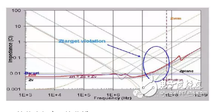
Figure 3: Cutoff Frequency Impedance Curve for VCCHIP
As previously explained, high-frequency noise in power supply traces is primarily generated by transient currents within the traces. The decoupling design guidelines for shared circuits with the highest cutoff frequency use impedance calculations based on the total transient current, which is an “over-design” requirement.
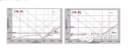
Figure 4: Changing Power Supply Sharing
In this case, you must calculate the target impedance curve based on the total transient current for the PCB decoupling project, equivalent to the maximum current consumption at the cutoff frequency of the power supply. In the case of sharing the VCC and VCCHIP power supply paths, you must use the VCC power supply cutoff frequency. Figure 3-A shows the impedance curve for the combined power supply path at the cutoff frequency of the core power supply decoupling. For the core power supply, the impedance curve is calculated using the total current (VCC + VCCHIP) flowing through the BGA balls or vias. You can then verify whether the result meets the target impedance of the individual power supply design guidelines.
Based on the same decoupling project as in Figure 4-A, Figure 4-B shows the impedance curve for the VCCHIP power supply. However, when generating this curve, only the current consumption and the number of BGA vias for VCCHIP need to be considered. As shown in Figure 4-B, the VCCHIP impedance curve meets the target impedance up to the cutoff frequency of the VCCHIP power supply. The final decoupling project must meet the target impedance at each frequency. If there are specific violations of the design targets, minimal adjustments can be made to optimize the decoupling project.
For similar situations, any power supply combination can be optimized using the VCC and VCCHIP examples.
When multiple FPGAs on a single PCB need to be powered from the same power supply, a similar approach can be used. For low-frequency solutions, the total current draw of the chips must be used; for high-frequency solutions, the current draw of one chip must be used. You can use the same number of capacitors for high-frequency decoupling of the other chips.
When compared to the solution obtained by the field analysis tool, if the spacing between the two FPGA chips is small, the high-frequency solution may result in a slight overdesign, as the field analysis tool takes the board layout into account. This may be because the chips are so close together that there is little capacitance to meet the required cutoff between the two chips. This also depends on the cutoff loop inductance of the capacitors as seen from the FPGA chip.
A common design trade-off is to create separate power planes and power different power rails from a single power supply, using filters to provide clean power to the power rails. In most cases, the filter is a ferrite bead connected between two power supplies on the board. As a rule, you can provide clean power to a single power supply network by following the following design guidelines.
■ When connecting a ferrite bead between two power supply networks, ensure that the mounting inductance is minimized.
■ Select the ferrite bead based on the characteristics listed below, ensuring that the current consumption of the power supply circuit is less than the bead’s rated current.
■ Sealing
■ Mounting size (0603, 0402, etc.)
■ Rated current
■ DC resistance
■ Impedance at the target frequency (10 MHz, 100 MHz, 1 GHz, etc.)
■ The frequency response of the ferrite bead’s equivalent RLC model must match the datasheet as closely as possible.
■ When performing AC analysis, be sure to include the ferrite bead model within the covered frequency range, along with the various capacitors selected to achieve the target impedance. When designing the capacitor’s equivalent RLC model, consider the mounting inductance as part of the model. If the AC analysis shows no peaks in the frequency band of interest (DC to 200 MHz), you can use ferrite bead isolation to provide clean power.
■ The PDN results obtained from the above simulation will definitely meet the target impedance requirements within the frequency band of interest.