
Skip to content
Andwin Circuits
  • Home
  • ProductsExpand
    • HDI multilayer PCB
    • Rigid Flex PCB
    • Flex pcb
    • Special PCBExpand
      • High Frequency PCBExpand
        • Rogers RO4350B PCB
        • Rogers RO4003 pcb
        • Rogers RO3003 PCB
        • Rogers 5880 PCB
        • DICLAD 527 PCB
        • Taconic TLX series
        • Taconic TLX-8 RF PCB
        • Taconic TLX-9 RF PCB
      • High speed pcbExpand
        • Megtron 6 High Speed PCB
        • TU-872 SLK Sp High Speed
      • High TG PCBExpand
        • SHENGYI SH260 PCB
        • ISOLA 370HR PCB
        • ISOLA IS410 PCB
        • ISOLA IS420 PCB
      • Heavy copper PCB
      • Copper coin pcb
      • Copper inlay PCB
    • Metal Core PCBExpand
      • Copper core pcb
      • Aluminum PCB
      • 2 Layers Aluminum PCB
      • Direct thermal MCPCB
      • 2 Layers Direct Thermal
    • Ceramic PCBExpand
      • DPC ceramic PCB
      • DBC ceramic PCB
      • Thick film Ceramic PCB
      • Al2O3 Alumina PCB
      • AIN ALN ceramic PCB
      • IGBT Ceramic PCB
  • ServiceExpand
    • PCB Assembly
    • Quick turn PCB assembly
    • PCBA conformal coating
  • IndustryExpand
    • Telecommunication
    • IoT and Wireless
    • Industrial Control
    • Thermal management
    • Power and Energy
    • IC test board
    • Automative
    • Medical
  • CapabilityExpand
    • Rigid PCB
    • Rigid flex PCB
    • Metal core PCB
    • PCB Assembly
  • TechnologyExpand
    • Blogs
    • Via in pad
    • PCB E-test
    • PCB stack up
    • MCPCB panelization
    • Controlled impedance PCB
  • AboutExpand
    • About us
    • Certification
    • Factory Tour
  • Contact
Andwin Circuits
Home / Five Key Benefits of PCB Plasma Treatment

Five Key Benefits of PCB Plasma Treatment

ByGrace July 31, 2025July 31, 2025

PCB plasma treatment is a surface treatment method for PCBs using plasma technology. Today, our editors will explain PCB plasma treatment in detail.

PCB plasma treatment uses high-energy plasma to clean, activate, and modify the surface of PCBs. The PCB is placed in a vacuum chamber to ensure a clean and stable environment. The desired gas (such as oxygen or nitrogen) is introduced into the chamber, and the plasma is formed by controlling the gas flow and pressure.

PCB plasma treatment excites gas molecules by heating or other means, ionizing them into a plasma state. When the PCB surface is exposed to the plasma, the plasma cleans, activates, and modifies the surface.

PCB plasma treatment allows for control of parameters such as plasma temperature, pressure, gas type, and treatment time to accommodate different PCB materials and treatment requirements. After treatment, the PCB undergoes post-treatment, which may include cleaning and drying, to ensure a long-lasting and stable surface treatment.

Plasma, a high-energy state consisting of ionized gas molecules and free electrons, can clean, activate, and modify the surface of PCBs. So what are the benefits of PCB plasma treatment?
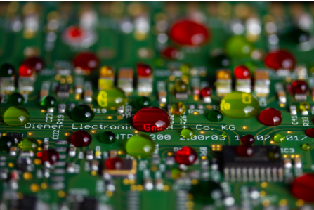
Contact us for PCB quote now |

The main functions of PCB plasma treatment are:

  1. Plasma can effectively remove organic contaminants, oxides, and other impurities from the PCB surface, leaving it clean.
  2. Plasma treatment activates the PCB surface, increasing its surface energy and improving the adhesion of coatings, bonding, or plating.
  3. Through plasma treatment, functional groups can be introduced to the PCB surface, changing the surface chemical properties and achieving specific surface functionalization.
  4. Plasma treatment can effectively remove the oxide layer on the PCB surface, improving the surface’s electrical properties and solderability.
  5. Compared to traditional chemical cleaning methods, PCB plasma treatment is generally more environmentally friendly and energy-efficient, reducing the discharge of chemical waste.

PCB plasma treatment technology has important applications in PCB manufacturing and soldering processes, improving the quality, reliability, and performance of PCBs. At the same time, it is important to select appropriate plasma treatment parameters based on the specific PCB material and process requirements to ensure optimal treatment results.

The above is the content sharing about PCB plasma treatment. I hope that the content compiled by the editor of Jieduobang can help you better understand PCB plasma treatment.

Contact us for PCB quote now |

Post Tags: #aluminum clad pcb#aluminum core pcb#aluminum core pcb led#aluminum pcb#assemble pcb#pcb plasma treatment

Post navigation

Previous Previous
What is the surface tension of a PCB?
NextContinue
What are the selection criteria for conformal coating on PCBs?

Search

Search

Products

  • HDI Multilayer PCB
  • Rigid Flex PCB
  • Flex pcb
  • High Frequency PCB
  • High speed pcb
  • Heavy copper PCB
  • Metal Core PCB
  • Ceramic PCB

Address

Andwin Circuits Co.,Limited
Email: sales@andwinpcb.com
Tel: +86 755 2832 9394
Fax:+86 755 2992  6717
ADD:1-2F-1217,HouDeQun Industrial park,
NanTing RD NO.56,ShaJing,BaoAn,Shenzhen 518104,GuangDong,China

Products

  • HDI Multilayer PCB
  • Rigid Flex PCB
  • Flex pcb
  • High Frequency PCB
  • High speed pcb
  • Heavy copper PCB
  • Metal Core PCB
  • Ceramic PCB

Technology

  • Blogs
  • Via in pad
  • PCB E-test
  • PCB stack up
  • Metal core PCB panelization
  • Controlled impedance PCB

CERTIFICATION

Certification >>


Copyright© 2003 - 2026 Andwin | All Rights Reserved | Powered by Andwin

Scroll to top
  • Home
  • Products
    • HDI multilayer PCB
    • Rigid Flex PCB
    • Flex pcb
    • Special PCB
      • High Frequency PCB
        • Rogers RO4350B PCB
        • Rogers RO4003 pcb
        • Rogers RO3003 PCB
        • Rogers 5880 PCB
        • DICLAD 527 PCB
        • Taconic TLX series
        • Taconic TLX-8 RF PCB
        • Taconic TLX-9 RF PCB
      • High speed pcb
        • Megtron 6 High Speed PCB
        • TU-872 SLK Sp High Speed
      • High TG PCB
        • SHENGYI SH260 PCB
        • ISOLA 370HR PCB
        • ISOLA IS410 PCB
        • ISOLA IS420 PCB
      • Heavy copper PCB
      • Copper coin pcb
      • Copper inlay PCB
    • Metal Core PCB
      • Copper core pcb
      • Aluminum PCB
      • 2 Layers Aluminum PCB
      • Direct thermal MCPCB
      • 2 Layers Direct Thermal
    • Ceramic PCB
      • DPC ceramic PCB
      • DBC ceramic PCB
      • Thick film Ceramic PCB
      • Al2O3 Alumina PCB
      • AIN ALN ceramic PCB
      • IGBT Ceramic PCB
  • Service
    • PCB Assembly
    • Quick turn PCB assembly
    • PCBA conformal coating
  • Industry
    • Telecommunication
    • IoT and Wireless
    • Industrial Control
    • Thermal management
    • Power and Energy
    • IC test board
    • Automative
    • Medical
  • Capability
    • Rigid PCB
    • Rigid flex PCB
    • Metal core PCB
    • PCB Assembly
  • Technology
    • Blogs
    • Via in pad
    • PCB E-test
    • PCB stack up
    • MCPCB panelization
    • Controlled impedance PCB
  • About
    • About us
    • Certification
    • Factory Tour
  • Contact
Search