Skip to content
Andwin Circuits
  • Home
  • ProductsExpand
    • HDI multilayer PCB
    • Rigid Flex PCB
    • Flex pcb
    • Special PCBExpand
      • High Frequency PCBExpand
        • Rogers RO4350B PCB
        • Rogers RO4003 pcb
        • Rogers RO3003 PCB
        • Rogers 5880 PCB
        • DICLAD 527 PCB
        • Taconic TLX series
        • Taconic TLX-8 RF PCB
        • Taconic TLX-9 RF PCB
      • High speed pcbExpand
        • Megtron 6 High Speed PCB
        • TU-872 SLK Sp High Speed
      • High TG PCBExpand
        • SHENGYI SH260 PCB
        • ISOLA 370HR PCB
        • ISOLA IS410 PCB
        • ISOLA IS420 PCB
      • Heavy copper PCB
      • Copper coin pcb
      • Copper inlay PCB
    • Metal Core PCBExpand
      • Copper core pcb
      • Aluminum PCB
      • 2 Layers Aluminum PCB
      • Direct thermal MCPCB
      • 2 Layers Direct Thermal
    • Ceramic PCBExpand
      • DPC ceramic PCB
      • DBC ceramic PCB
      • Thick film Ceramic PCB
      • Al2O3 Alumina PCB
      • AIN ALN ceramic PCB
      • IGBT Ceramic PCB
  • ServiceExpand
    • PCB Assembly
    • Quick turn PCB assembly
    • PCBA conformal coating
  • IndustryExpand
    • Telecommunication
    • IoT and Wireless
    • Industrial Control
    • Thermal management
    • Power and Energy
    • IC test board
    • Automative
    • Medical
  • CapabilityExpand
    • Rigid PCB
    • Rigid flex PCB
    • Metal core PCB
    • PCB Assembly
  • TechnologyExpand
    • Blogs
    • Via in pad
    • PCB E-test
    • PCB stack up
    • MCPCB panelization
    • Controlled impedance PCB
  • AboutExpand
    • About us
    • Certification
    • Factory Tour
  • Contact
Andwin Circuits
Home / How to master multilayer PCBs?

How to master multilayer PCBs?

ByGrace August 6, 2025August 6, 2025

When hardware engineers first encounter multilayers PCBs,It is easy to feel overwhelmed.Ten or eight layers are common,and the lines resemble a spiderweb.

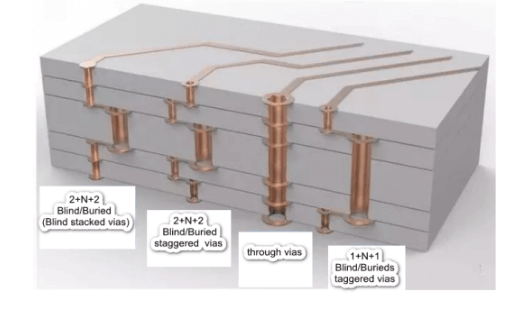
Another ways to think about it is to use a 3D diagram to show the internal structure of various stacked PCB diagrams.This is much easier to understand.

How to Master Multilayer PCBs?

The most important part of an HDI board is the vias.

The wiring process for multilayer PCBs is no different from single-layer or multilayer boards;the biggest difference is the via process.

The lines are etched drilled, and then copper plated.Hardware developers understand this and won’t elaborate.

Multilayer PCBs typically use via:a first-order board a second-order board,and then a third-order stacked via.Higher orders,such as third-order board,interconnect anyone layer,which is typically very expensive and rarely discussed.Generally speaking,8 bit microcontroller products use 2-layer through-hole board;32-bit MCU-lever smart hardware uses 4-and 6-layer through-hole boards;Linux and Android-lever smart hardware uses 6-to 8-layer 1-step HDI board;compact product such as smartphones typically use 8-to 10-layer 2-step HDI boards.

8-layer 2-step HDI,Qualcomm Snapdragon 624

The most common through-hole pattern

There is only one type of hole from the first to the last.Whether it’s for external or internal traces,the hole is perforated.This is called a through-hole board.

The number of layer in a through-hole board doesn’t matter.Generally,everyone uses 2-layer through-hole board.Many switch and military boards have 20 layer,but they still use through-holes.

Board holes are drilled and copper is plate to form the traces.

It should be noted that the inner diameter of through-holes is typically 0.2mm,0.25mm,and 0.3mm ,but 0.2mm is generally much more expensive than 0.3mm.Because the drill bit is too thin and easily breaks,drilling speed is slow,The increased time and cost of the drill bit are reflected in the increased price of circuit board.

Laser vias in HDI boards

This photo shows a 6-layer,1-laminate structure diagram for ordering HDI board.Both layers on the surface have laser holes with an inner diameter of 0.1mm.The inner layer has a mechanical hole equivalent to a 4-layer through-hole board,and the outer layer is covered with 2 layers.The laser can only penetrate fiberglass board,not copper metal.Therefore, the laser can only penetrate fiberglass board, not copper metal.Therefore,the holes on the outer surface do not affect other internal wiring.The laser perforation is then followed by copper plating,and the laser holes are formed through the holes.

2-Sequential HDI Board,Two sets of laser vias.

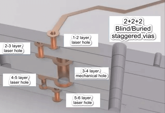
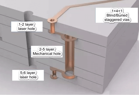
This is a 6-layer,2-stage staggered HDI board.Typically,6 layers and 2 layers are used,with 8 layers and 2 layers being the most common.In this case,the larger number of layers corresponds to the same number of so-called 2-stage laser holes,meaning there are two sets of laser holes,Why the staggering?Because the copper plating is not satisfactory and the holes are empty,laser holes cannot be directly above the holes.Instead,they must be staggered a certain distance and then laser holes are ceated one layer at a time.

6-layer 2-stage HDI=4-layer 1-stage HDI+2 layers

8-layer 2-stage HDI=6-layer 1-stage HDI+2 layers

Stacked via boards are technically complex and more expensive

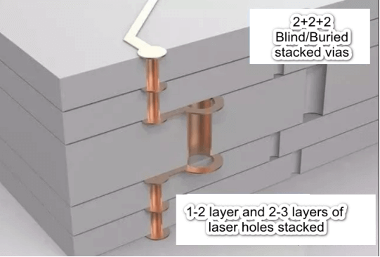
The laser holes in staggered via board overlap,making the circuit more compact.The inner laser holes require plating and filling,and then the outer laser holes need to be created.The price is higher the staggered vias.

Super expensive any-layer interconnect boards,multi-layer laser stacks.

Each layer has laser holes,allowing each layer to be connected together. you can use wires as needed and drill holes as needed.However,it is over 10 times more expensive than regular through- hole boards!

For this reason,only iPhones are willing to use them.Other phone brands have not heard of any single-layer interconnect boards.

Let’s take a closer look and compare them again.Pay attention to the hole size and whether the pads of the holes are closed or open.

Contact us for PCB quote now |
Post Tags: #multilayer pcb#pcb design

Post navigation

Previous Previous
How Signals Propagate in PCBs
NextContinue
How to Effectively prevent Excessive PCB corrosion

Search

Search

Products

  • HDI Multilayer PCB
  • Rigid Flex PCB
  • Flex pcb
  • High Frequency PCB
  • High speed pcb
  • Heavy copper PCB
  • Metal Core PCB
  • Ceramic PCB

Address

Andwin Circuits Co.,Limited
Email: sales@andwinpcb.com
Tel: +86 755 2832 9394
Fax:+86 755 2992  6717
ADD:1-2F-1217,HouDeQun Industrial park,
NanTing RD NO.56,ShaJing,BaoAn,Shenzhen 518104,GuangDong,China

Products

  • HDI Multilayer PCB
  • Rigid Flex PCB
  • Flex pcb
  • High Frequency PCB
  • High speed pcb
  • Heavy copper PCB
  • Metal Core PCB
  • Ceramic PCB

Technology

  • Blogs
  • Via in pad
  • PCB E-test
  • PCB stack up
  • Metal core PCB panelization
  • Controlled impedance PCB

CERTIFICATION

Certification >>


Copyright© 2003 - 2026 Andwin | All Rights Reserved | Powered by Andwin

Scroll to top
  • Home
  • Products
    • HDI multilayer PCB
    • Rigid Flex PCB
    • Flex pcb
    • Special PCB
      • High Frequency PCB
        • Rogers RO4350B PCB
        • Rogers RO4003 pcb
        • Rogers RO3003 PCB
        • Rogers 5880 PCB
        • DICLAD 527 PCB
        • Taconic TLX series
        • Taconic TLX-8 RF PCB
        • Taconic TLX-9 RF PCB
      • High speed pcb
        • Megtron 6 High Speed PCB
        • TU-872 SLK Sp High Speed
      • High TG PCB
        • SHENGYI SH260 PCB
        • ISOLA 370HR PCB
        • ISOLA IS410 PCB
        • ISOLA IS420 PCB
      • Heavy copper PCB
      • Copper coin pcb
      • Copper inlay PCB
    • Metal Core PCB
      • Copper core pcb
      • Aluminum PCB
      • 2 Layers Aluminum PCB
      • Direct thermal MCPCB
      • 2 Layers Direct Thermal
    • Ceramic PCB
      • DPC ceramic PCB
      • DBC ceramic PCB
      • Thick film Ceramic PCB
      • Al2O3 Alumina PCB
      • AIN ALN ceramic PCB
      • IGBT Ceramic PCB
  • Service
    • PCB Assembly
    • Quick turn PCB assembly
    • PCBA conformal coating
  • Industry
    • Telecommunication
    • IoT and Wireless
    • Industrial Control
    • Thermal management
    • Power and Energy
    • IC test board
    • Automative
    • Medical
  • Capability
    • Rigid PCB
    • Rigid flex PCB
    • Metal core PCB
    • PCB Assembly
  • Technology
    • Blogs
    • Via in pad
    • PCB E-test
    • PCB stack up
    • MCPCB panelization
    • Controlled impedance PCB
  • About
    • About us
    • Certification
    • Factory Tour
  • Contact
Search