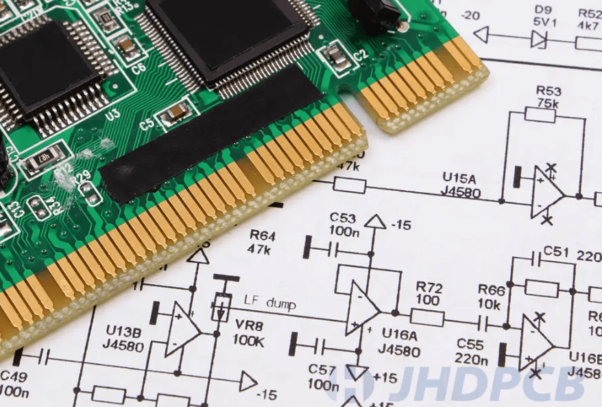
PCB design and Process Specification
As a PCB layout engineer,printed circuit board(PCB)design is your bread and butter.Not only must you diligently”draw the line”,but you must also maintain a holistic understanding and understand the entire process.Generally speaking,PCB design consist of three main parts:preliminary preparation,pcb design,and post-processing.
I.Preliminary Preparation
1.Clarify the design goals,select the component types,confirm the overall plan,and produce a written design plan.
2.Prepare schematic and PCB footprint libraries for the components.Each component must have a footprint.If the basic library doesn’t have a footprint,you’ll have to draw it yourself.You can use footprint generation software for this.It is important to ensure that the footprint is placed in the designated directory.
II.PCB design
This part is the core of PCB design.However,if any problems arise in the initial plan,it will create many obstacles later on.Therefore,a good plan is half the battle.The next step is to proceed step by step with the design.
1.Schematic Design
Schematic design isn’t a very labor-intensive task,but its important is undeniable.A correct schematic guarantees the functionality of the entire circuit board.
2.Create a Schematic Netlist
After creating the schematic,a netlist must be generated for importing into PCB design software,If using Cadence,the generate netlist file contains three files:pstxnet.dat,pstxprt.dat, and pstchip.dat.
3.Create a Mechanical Design Drawing
Set the PCB outline and height restriction,generate a new mechanical drawing file,and save it to the specified directory.
4.Read the Schematic Netlist
Read the schematic netlist into PCB software such as Allegro
5.Set Basic PCB information
Before beginning layout and routing ,be sure to set the pcb layer,grid spacing,color,and design constraints.
6.PCB layout
Expect for very simple schematics,manual layout is recommended based on the functional distribution of the schematic.
7.PCB routing
Manual rotuing takes longer but is more precise and meets actual requirements.Automatic routing is faster but used more overriding.Manual routing or a combination of both methods is generally recomended
8.Test Point Placement
Place voltage test points in appropriate locations to facilitate quick testing and confirmation after the board is built
9.Top and bottom copper planing
This step is optional,but it is performed on almost all mature designs.It not only reinforces the board and prevent warping,but also enhances the board’s shielding performance and improves its anti-interference capabilities.
10. Constraint rule check
If you designed some constraints before layout and routing,you should now check the constraint table to ensure that all routing and other aspects comply with the rules.A PCB design checklist can be created in three steps:
①. Data Input
①. Data Input
Check whether all the data received during the process is complete (including schematics, *.brd files, bill of materials, PCB design specifications, PCB design or change requirements, standardization requirements, process design specifications, etc.).
Confirm that the PCB template is up to date.
Check whether the clock component layout is reasonable.
Confirm that the component positioning on the template is correct.
Check whether the PCB design specifications PCB design or change requirement,and standardization requirements are clear.
Confirm that the prohibited placement areas and routing zones indicated in the outline drawing are reflected on the pcb template.
Compare the outline drawing to confirm that the dimensions and tolerances marked on the PCB are correct,and that the plated and non-plated holes are defined accurately.
After confirming the accuracy of the PCB template,it is best to lock the structure file to prevent accidental movement.
②. Post-Layout Review
1.Component Inspection
Confirm that all component footprints are consistent with the company’s unified library and that the footprint library has been updated (use ViewLog to check the run results). If not, be sure to update the Symbols.
Confirm that the motherboard and daughterboard, and the single board and backplane, have corresponding signals and positions, the connector orientation and silkscreen markings are correct, and that the daughterboard has anti-misinsertion measures to prevent interference between the daughterboard and the motherboard components.
Check that the components are 100% placed.
Enable place-bound on the top and bottom layers of the device to check whether the DRC allows for overlap.
Check that the mark points are sufficient and necessary.
Heavier components should be placed near PCB support points or edges to reduce PCB warpage.
Confirm that all device footprints are consistent with the company’s unified library and that the footprint library has been updated (use ViewLog to check the run results). If there are any discrepancies, be sure to update the symbols.
For the motherboard and daughterboard, and the single board and backplane, confirm that the signals and positions correspond, the connector orientation and silkscreen markings are correct, and that the daughterboard has anti-misinsertion measures, and that there is no interference between the components on the daughterboard and the motherboard.
Check that the components are 100% placed.
Enable the place-bound function on the top and bottom layers of the device to check whether the DRCs for overlap allowable.
Check that the number of marks is sufficient and necessary.
Heavier components should be placed near PCB support points or edges to reduce PCB warpage.
After placement, structurally related components should be locked to prevent accidental movement.
Within a 5mm radius around the pressfit socket, no components taller than the front of the socket are allowed, and no components or solder joints are allowed on the back.
Confirm that the device layout meets process requirements (focus on BGA, PLCC, and surface mount sockets).
For components in metal housings, pay special attention to avoid contact with other components and ensure adequate clearance.
Place interface-related components as close to the interfaces as possible, and backplane bus drivers as close to the backplane connectors as possible.
Check whether the chip components on the wave soldering surface have been converted to wave solder packages.
Check whether there are more than 50 manual solder joints.
For components that are axially mounted high on the PCB, consider horizontal mounting. Leave space for horizontal placement. Consider mounting methods, such as mounting pads for crystal oscillators.
For components that require heat sinks, ensure adequate clearance from other components and pay attention to the height of key components within the heat sink area.
2.Functional Inspection
Check whether the digital and analog circuits on the mixed-signal board are separated during layout, and whether the signal flow is reasonable.
Place the A/D converter across the analog-to-digital partition.
Check whether the clock device layout is reasonable.
Check whether the high-speed signal device layout is reasonable.
Are the termination components properly placed? (Source-end matching resistors should be placed at the signal driver; intermediate matching resistors should be placed in the middle; and terminal matching resistors should be placed at the signal receiver.)
Signal lines use planes of different voltage levels as reference planes. When crossing plane dividers, are the connecting capacitors between reference planes close to the signal routing area?
Is the protection circuit layout appropriate and facilitates division? Is the fuse for the board power supply placed near the connector, with no circuit components in front of it?
Confirm that circuits for strong and weak signals (with a power difference of 30dB) are routed separately.
Is the number and placement of decoupling capacitors for IC devices appropriate?
Are components that may affect EMC testing placed according to design guidelines or referenced by successful practices? For example, the reset circuit on the panel should be slightly closer to the reset button.
3.Heat
Heat-sensitive components (including liquid dielectric capacitors and crystal oscillators) should be kept as far away from high-power components, heat sinks, and other heat sources as possible.
Does the layout meet thermal design requirements and heat dissipation paths (performed according to the process design documents)?
4.Power Supply
Is the IC power supply too far from the IC?
Is the layout of the LDO and surrounding circuits appropriate?
Is the layout of surrounding circuits such as the module power supply appropriate?
Is the overall layout of the power supply appropriate?
5.Rule Settings
Have all simulation constraints been correctly added to the Constraint Manager?
Have the physical and electrical rules been correctly set (pay attention to the constraints for the power and ground nets)?
Is the spacing between test vias and test pins sufficient?
Does the thickness and layout of the stackup meet design and processing requirements?
Have the impedances of all differential lines with characteristic impedance requirements been calculated and controlled using rules?
③. Post-Layout Inspection
6.Digital and Analog
Have the routing of digital and analog circuits been separated, and is the signal flow reasonable?
If A/D, D/A, and similar circuits have split ground planes, do signal lines between circuits run over the bridge point between the two grounds (except for differential lines)?
Signal lines that must cross the gap between split power supplies should reference a complete ground plane.
If using a ground plane design with partitioning but not splitting, ensure that digital and analog signals are routed separately.
7.Clock and High-Speed Sections
Is the impedance of high-speed signal lines consistent across all layers?
Are high-speed differential signal lines and similar signal lines routed in equal lengths, symmetrically, and parallel to each other as closely as possible?
Confirm that clock lines are routed on inner layers as much as possible.
Confirm that clock lines, high-speed lines, reset lines, and other highly radiative or sensitive lines are routed according to the 3W principle as much as possible.
Are there no bifurcated test points on clock, interrupt, reset signals, 100M/1G Ethernet, and high-speed signals?
Does the 10H (H is the height of the signal line from the reference plane) distance between low-level signals such as LVDS and TTL/CMOS signals meet the required 10H (H is the height of the signal line from the reference plane) as much as possible?
Avoid routing clock lines and high-speed signal lines through densely packed vias or between device pins.
Check whether the clock lines meet SI constraints (clock signal routing ensures minimal vias, short routing, and continuous reference planes, with the primary reference plane preferably being GND; if the GND primary reference plane layer is changed during layer switching, GND vias are located within 200 mils of the vias; if the primary reference planes are changed at different voltage levels during layer switching, are decoupling capacitors located within 200 mils of the vias).
Check whether differential pairs, high-speed signal lines, and various bus lines meet SI constraints.
8.EMC and Reliability
For crystal oscillators, check whether a ground plane is laid underneath them; check whether signal lines are prevented from crossing between device pins; and check whether signal lines are prevented from crossing between device pins for high-speed sensitive devices.
Signal traces on the board should avoid sharp or right angles (generally, continuous turns should be made at 135 degrees. RF signal traces should preferably use rounded or calculated angled copper foil).
For double-sided boards, check whether high-speed signal lines are routed closely to their return ground lines. For multi-layer boards, check whether high-speed signal lines are routed as close to the ground plane as possible.
For signal lines on adjacent layers, route them perpendicularly as much as possible.
Avoid signal lines passing under power modules, common-mode inductors, transformers, and filters.
Try to avoid long, parallel high-speed signal lines on the same layer.
Check the board edges and the edges separating the digital, analog, and protective ground planes for shielded vias; are multiple ground planes connected by vias? Is the via distance less than 1/20 of the wavelength of the highest-frequency signal?
Check whether the signal traces corresponding to surge suppressors are short and thick on the surface layers.
Confirm that there are no isolated islands in the power and ground layers, no excessive slots, no long ground plane cracks caused by oversized via isolation pads or densely packed vias, and no thin strips or narrow channels.
Check whether ground vias are placed where signal lines frequently cross layers (at least two ground planes are required).
9.Power and Ground
If the power/ground planes are split, avoid crossing high-speed signals on the split reference planes.
Confirm that the power and ground planes can carry sufficient current. Check that the number of vias meets the current carrying requirements (estimated as follows: 1A/mm trace width for 1oz copper thickness on outer layers, 0.5A/mm trace width on inner layers, and double the current for short traces).
For power supplies with special requirements, check that the voltage drop requirements are met.
To reduce the edge radiation effect of the plane, adhere to the 20H principle between the power and ground planes as much as possible (if conditions permit, the greater the indentation of the power plane, the better).
If there is a ground split, check that the split ground planes do not form loops.
Are different power planes on adjacent layers placed without overlapping?
Is the isolation between the protective ground, -48V ground, and GND greater than 2mm?
Is the -48V ground only a return path for the -48V signal and not connected to other grounds? If this is not possible, please explain the reason in the comments column.
Is a 10-20mm protective ground plane installed near the connector panel, and is the space between each layer connected using double rows of staggered holes?
Does the spacing between power cables and other signal lines meet safety regulations?
10.Prohibited Areas
Traces, copper foil, and vias that could cause short circuits should not be installed under metal housing components and heat sinks.
Traces, copper foil, and vias that could cause short circuits should not be installed around mounting screws or washers.
Are there any areas reserved for routing in the design requirements?
The spacing between non-metallized holes and traces and copper foil on inner layers should be greater than 0.5mm (20 mils), and 0.3mm (12 mils) on outer layers. The spacing between the inner layers of the board extraction wrench shaft hole and traces and copper foil should be greater than 2mm (80 mils).
The recommended spacing between copper foil and traces and the board edge is greater than 2mm, with a minimum of 0.5mm.
The spacing between the inner ground layer copper foil and the board edge is 1-2mm, with a minimum of 0.5mm.
11.Pad Leading
For chip components (packages 0805 and smaller) with two pads, such as resistors and capacitors, the traces connecting to the pads should ideally be symmetrically routed from the center of the pads. The traces connecting to the pads must be the same width. This rule does not apply to traces with a width less than 0.3mm (12 mils).
For pads connected to wider traces, a narrow trace transition is recommended (packages 0805 and smaller).
Traces should be routed from both ends of the pads for components such as SOIC, PLCC, QFP, and SOT.
12.Silkscreen
Check whether the component part number is missing and whether the position correctly identifies the component.
Check whether the component part number complies with company standards.
Confirm the correct pinout order, pin 1 designation, polarity marking, and connector orientation.
Check whether the motherboard and daughterboard orientation markings match.
Check that the backplane is correctly labeled with slot names, slot numbers, port names, and housing orientation.
Confirm that the silkscreen design requirements are correctly applied.
Confirm that the anti-static and RF board labels (for RF boards) are in place.
13.Coding/Barcode
Confirm that the PCB coding is correct and complies with company specifications.
Confirm that the PCB coding position and layer are correct for the board (it should be in the upper left of side A, on the silkscreen layer).
Confirm that the PCB coding position and layer are correct for the backplane (it should be in the upper right of side B, on the outer copper foil layer).
Confirm that the barcode laser-printed white silkscreen marking area is present.
Confirm that there are no connecting lines or vias larger than 0.5mm below the barcode frame.
Confirm that no components taller than 25mm are within 20mm of the white silkscreen barcode area.
14.Vias
On the reflow soldering surface, vias cannot be designed on pads (normally open window)
The spacing between vias and pads should be greater than 0.5mm (20mil), and the spacing between vias covered with green ink and pads should be greater than 0.1mm (4mil). To do this, enable Same Net DRC, check the DRC, and then disable Same Net DRC.
Vias should not be arranged too closely to avoid causing large breaks in the power and ground planes.
The drilled via diameter should ideally be no less than 1/10 of the board thickness.
15.Process
Is the component placement rate 100%? Is the routing pass rate 100%? (If it is not 100%, please indicate this in the notes.)
Have dangling lines been minimized? Have any remaining dangling lines been individually verified?
Have the process issues reported by the process department been carefully reviewed?
16.Large Copper Foil Areas
For large copper foil areas on the top and bottom, unless otherwise required, use a grid copper mesh (diagonal mesh for single boards, orthogonal mesh for backplanes, with a line width of 0.3mm (12 mil) and a spacing of 0.5mm (20 mil)).
Component pads in large copper foil areas should be designed as decorative pads to prevent cold solder joints. If current requirements are met, consider widening the ribs of the decorative pads before considering full connection.
When routing copper over large areas, avoid dead copper (islands) with no network connection.
For large copper foil areas, also pay attention to illegal connections and unreported DRCs.
17.Test Points
Ensure that there are sufficient test points for various power and ground circuits (at least one test point for every 2A of current).
Confirm that nets without test points are confirmed to be streamlined.
Confirm that test points are not set on plug-ins that will not be installed during production.
Confirm that test vias and test pins are fixed (applicable to board modifications where the test bed remains unchanged).
18.DRC
The spacing rules for test vias and test pins should first be set to the recommended distances. Check the DRC. If DRC still exists, recheck the DRC using the minimum distance setting.
Enable constraints, update the DRC, and check for any unacceptable errors.
Confirm that the DRC has been adjusted to the minimum. If DRC cannot be eliminated, recheck each one.
19.Optical Fiducials
Confirm that optical Fiducials are present on the PCB surface with mounted components.
Confirm that the optical Fiducials are not overprinted (silk screen and copper traces).
The background of the optical Fiducials must be consistent. Confirm that the center of the optical Fiducials used throughout the board is ≥5mm from the edge.
Confirm that the coordinates of the optical Fiducials for the entire board have been assigned (it is recommended that the optical Fiducials be placed as components), and that the values are integers in millimeters.
For ICs with a pin center pitch of less than 0.5mm and BGA components with a center pitch of less than 0.8mm (31 mils), optical alignment points should be placed near the component diagonals.
20.Solder Mask Inspection
Confirm that all pads with special requirements are properly windowed (pay particular attention to hardware design requirements).
Are the vias under the BGA properly treated as oil-filled vias?
Are small windows or oil-filled vias used for vias other than test vias?
Check that the optical alignment points’ openings avoid exposed copper and wires.
For components such as power chips and crystal oscillators that require copper foil for heat dissipation or grounding, check that copper foil is properly covered and properly windowed. Components secured by solder should have green solder paste to prevent large-area solder spread.
21.Drill Map
Check that the PCB thickness, number of layers, silkscreen color, warpage, and other technical specifications in the notes are correct.
Check the layer names, stackup order, dielectric thickness, and copper foil thickness in the stackup diagram. Is impedance control required and accurately described? Do the layer names in the stackup diagram match the photoresist file names?
Disable the Repeat code setting in the setup sheet. Set the drilling accuracy to 2-5.
Check whether the hole table and drill file are up to date (regeneration is required when holes are modified).
Check whether the hole table contains any unusual hole diameters. Check whether the hole diameters for press-fit components are correct. Check whether the hole diameter tolerances are correctly marked.
Check whether vias that require plug holes are listed separately and labeled “filled vias.”
22.Photoresistance
When exporting photoresist files, use RS274X format if possible, and set the accuracy to 5:5.
Check whether art_aper.txt is up to date (RS274X is not required).
Check whether the output photoresist log file contains any abnormality reports.
Confirm the edges and islands of the negative layer.
Use a photolithography inspection tool to check whether the photolithography file matches the PCB (use a comparison tool for comparison if modifying the board).
23.Complete File Set
PCB File: Product Model_Specifications_Board Code_Version Number.brd.
Backplane Liner Design File: Product Model_Specifications_Board Code_Version Number-CB[-T/B].brd.
PCB Processing File: PCB Coding.zip (Contains the photolithography files, aperture table, drill files, and ncdrill.log for each layer; paneling also requires the paneling *.dxf file provided by the process). The backplane also requires the liner file: PCB Coding-CB[-T/B].zip (Contains drill.art, *.drl, and ncdrill.log).
Process Design File: Product Model_Specifications_Board Code_Version Number-GY.doc.
SMT coordinate file: Product Model_Specifications_Board Code_Version Number – SMT.txt (When exporting the coordinate file, make sure to select Body Center. Symbol Origin can only be selected if the origin of all SMD component libraries is confirmed to be at the component center).
PCB board structure file: Product Model_Specifications_Board Code_Version Number – MCAD.zip (Contains .DXF and .EMN files provided by the structural engineer).
Test file: Product Model_Specifications_Board Code_Version Number – TEST.ZIP (Contains testprep.log and untest.lst or *.drl test point coordinate files).
Archived drawing file: Product Model Specifications – Board Name – Version Number.pdf (Includes: cover, first page, silkscreen for each layer, wiring for each layer, drill pattern, and backplane with backing board drawing).
24.Standardization
Confirm that the cover and first page information is correct.
Confirm that the drawing sequence (corresponding to the order of each PCB layer) is correct.
Confirm that the PCB code on the drawing frame is correct.
ICZOOM (www.iczoom.com) is a fast-matching component trading platform and a one-stop component procurement and integrated supply chain service platform. We specialize in providing electronic industry internet services to small and medium-sized businesses, including matching services, order matching, consignment purchasing, customs clearance and inspection, software customization, smart warehousing, smart logistics, and supply chain finance.
III. Post-Processing
- Adjusting the Text on the Board
Add and adjust the silkscreen, and add necessary prompts and company logos to the board.
- Outputting the Gerber File
Once the correct Gerber file is generated, it can be sent to the plate manufacturer for processing.
- Document Archiving
Common reports include: component lists, board interface wiring diagrams, and printed schematics and PCB layouts.