
Metal Core PCB for Electric Vehicle (EV) Charging Systems: Design Guidelines and Thermal Management
EV charging stations are tough on PCBs – high currents, sustained heat, outdoor temperature swings from -40°C to +85°C. Standard FR4 just doesn’t cut it for power conversion modules. Metal Core PCBs have become the go-to solution because they pull heat out of power devices and dump it into the chassis or heatsink. This guide covers the practical side of designing MCPCBs for Level 2 and DC fast chargers – material selection, thermal interface design, DFM rules, and what actually works in production.
Why Metal Core PCB Matters for EV Charging Applications
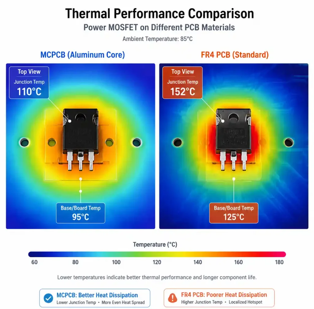
FR4 boards struggle with heat in EV charging power electronics. A 150kW DC fast charger’s rectifier, PFC stage, and DC-DC converter generate serious heat. Mount IGBTs or SiC MOSFETs on FR4 and junction temps spike – efficiency drops, reliability suffers.
MCPCBs fix this by swapping the FR4 core for an aluminum or copper base plate. The metal substrate acts as an integrated heat spreader, pulling heat away from power components to the heatsink. For outdoor chargers running in harsh environments, that thermal advantage directly translates to longer MTBF.
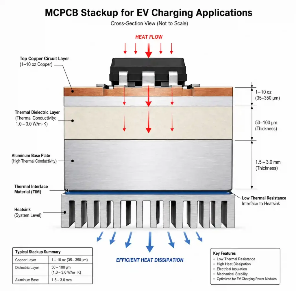
The dielectric layer between the copper circuit and metal base is engineered for both thermal conduction and electrical isolation. Typical thermal conductivity runs 1.5 W/m·K for standard MCPCB up to 8 W/m·K for high-performance variants. FR4’s through-plane thermal conductivity? Only 0.3 W/m·K. That’s why MCPCBs can cut junction-to-case thermal resistance by 60-80% in power module layouts.
Critical Design Parameters for EV Charging MCPCBs
Thermal Conductivity and Dielectric Thickness
The dielectric’s thermal conductivity determines how efficiently heat moves from the copper trace to the metal base. Match dielectric performance to your power density – don’t overspec if you don’t need it.
| Application | Power Density | Recommended Thermal Conductivity | Dielectric Thickness | Breakdown Voltage |
|---|---|---|---|---|
| AC-DC rectifier (3.3-7.2kW) | 50-80 W/in² | 1.5-2.0 W/m·K | 75-100 μm | 2.5-3.0 kV |
| DC-DC converter (22kW) | 100-150 W/in² | 3.0-4.0 W/m·K | 50-75 μm | 3.0-4.0 kV |
| DC fast charger module (≥150kW) | 150-250 W/in² | 6.0-8.0 W/m·K | 50 μm | 4.0-5.0 kV |
| LED indicator and HMI | 10-30 W/in² | 1.5-2.0 W/m·K | 100 μm | 2.0 kV |
For a 22kW Level 2 charger, 3.0 W/m·K dielectric at 75 μm gives you adequate isolation for 400V DC bus while keeping junction temps under 125°C. Thinner dielectrics transfer heat better but need careful clearance design per IPC-2221 voltage spacing rules.
Copper Thickness and Trace Width
EV charging circuits carry 10A to 400A continuous depending on charging level. MCPCB copper thickness ranges from 1 oz (35 μm) up to 10 oz (350 μm) for power traces. For high-current designs, thick copper PCBs with 6 oz or more provide the current-carrying capacity needed for 150A+ DC bus applications.
For a 150A DC output bus on a fast charger, you need at least 4 oz copper with 15-20mm trace width to keep temp rise under 30°C at 85°C ambient. That assumes the board is mounted with thermal interface material (TIM) to a heatsink and the aluminum base is 1.5-3.0mm thick.
Current capacity on MCPCB differs from FR4 because the metal base sinks heat. Per IPC-2152 with thermal backing, a 10mm trace in 4 oz copper on MCPCB handles roughly 80-100A – compared to 50-60A on FR4 with the same geometry.
Material Selection: Aluminum vs Copper Base
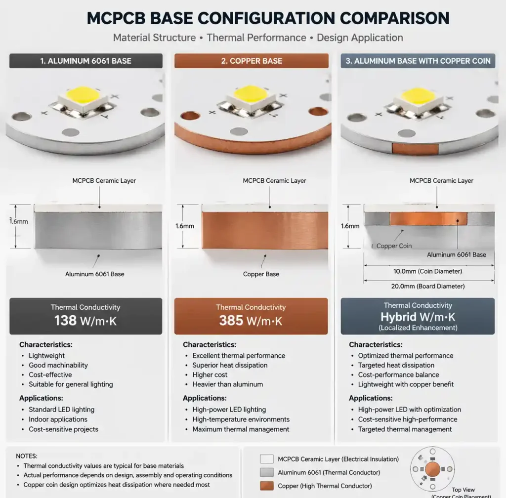
Most EV charging MCPCBs use aluminum for cost and weight reasons. Aluminum 5052 or 6061 alloys are standard, 1.0mm to 3.0mm thick. Copper base offers 2-3× better thermal conductivity but costs 3-5× more and adds significant weight. For a detailed comparison, see our guide on aluminum PCB vs metal core PCB for heat dissipation and material selection.
| Base Material | Thermal Conductivity | Typical Thickness | CTE (ppm/°C) | Relative Cost | Best Use Case |
|---|---|---|---|---|---|
| Aluminum 5052 | 138 W/m·K | 1.5-2.0 mm | 23.8 | 1× | Standard AC-DC, DC-DC converters |
| Aluminum 6061 | 167 W/m·K | 1.5-3.0 mm | 23.6 | 1.2× | High-reliability outdoor installations |
| Copper base | 385 W/m·K | 1.0-1.5 mm | 17.0 | 4-5× | Ultra-high power density (>200 W/in²) |
| Aluminum + copper coin | 138/385 W/m·K | 2.0mm Al + 0.5mm Cu coin | Mixed | 2-2.5× | Localized hotspot management |
For a typical 22kW Level 2 charger, aluminum 6061 at 2.0mm gives the best balance of thermal performance, mechanical strength, and cost. The aluminum base should be anodized or chromate conversion coated for corrosion resistance in outdoor environments.
Copper base is only justified when power devices are densely packed or when you need very low thermal resistance to meet automotive reliability targets (AEC-Q). A hybrid approach – aluminum base with embedded copper coins directly under high-dissipation components – gives you localized thermal improvement without the full copper cost.
Design Rules and Layer Stackup
Single Layer MCPCB Stackup
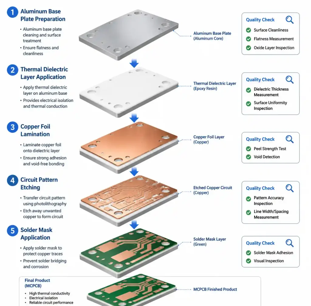
Most EV charging power modules use single-layer MCPCBs – components on one side, metal base on the other as heatsink interface. Stackup from top: copper circuit layer (1-10 oz), dielectric insulation (50-100 μm, thermally conductive), aluminum or copper base (1.0-3.0 mm).
Clearance and Creepage for High Voltage
IPC-2221 calls for minimum clearance based on working voltage and pollution degree. For 400V DC outdoor systems (Pollution Degree 3), minimum clearance is 2.5mm uncoated, 1.6mm conformally coated.
EV charging designs often follow automotive standards like ISO 6469 or UL 2202, which may require larger creepage. Our conservative rule for 400V DC bus routing on MCPCB: 3.0mm trace-to-trace, 4.0mm trace-to-edge when the metal base is grounded.
Thermal Via Design
MCPCBs conduct heat primarily through the dielectric to the metal base – thermal vias aren’t the primary path. But they can help spread heat locally within the copper layer. Don’t drill through the metal base – that compromises structural integrity and thermal continuity.
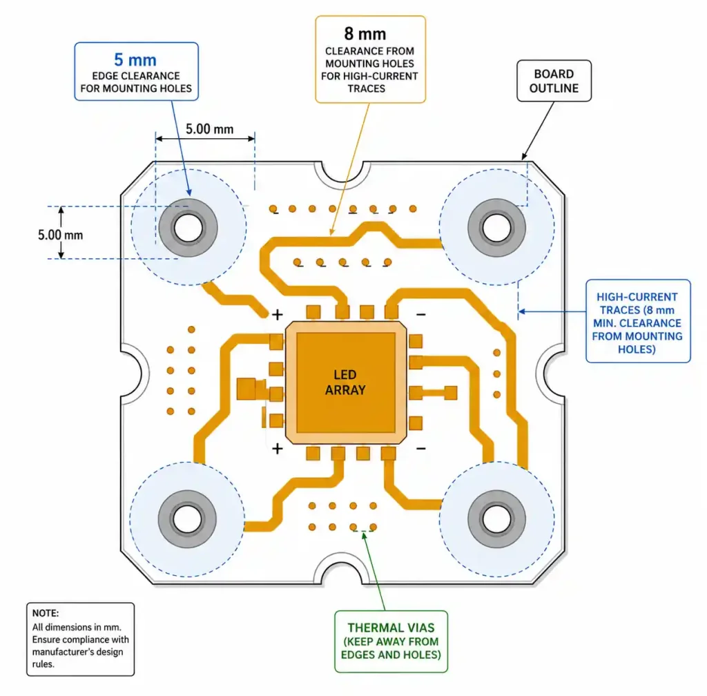
If you need vias (e.g., gate signals in a half-bridge), follow blind and buried via design rules for proper aspect ratio control. Use plated-through holes at 0.3-0.5mm diameter with at least 5mm edge clearance. Consider a hybrid approach where the MCPCB segment is single-layer, interconnected to a small FR4 multilayer control section.
DFM Considerations and Manufacturing Pitfalls
Mounting Holes and Mechanical Stress
EV charging modules see vibration in transit and thermal cycling in operation. Mounting holes need careful placement to avoid stress concentration in the dielectric.
Put mounting holes at least 5mm from board edges and 8mm from high-current traces. Use non-plated mounting holes with 0.5mm extra diameter for thermal expansion clearance. If you need electrically connected mounting holes, specify plated-through with 0.2mm annular ring minimum – but know it adds cost and limits thermal performance.
Solder Mask and Thermal Interface
Most MCPCBs have LPI solder mask on the component side, bare metal base on the back. The aluminum surface must be flat and clean for good TIM contact. Specify flatness tolerance ±0.1mm and RA roughness <1.6 μm.
For thermal grease, chemically clean or lightly abrade the aluminum. For phase-change TIM or thermal pads, anodizing improves adhesion but adds slight thermal resistance (0.01-0.02 K·in²/W).
Component Footprint Design
Power packages like TO-247, TO-220, and D2PAK have large thermal pads. On MCPCBs, the footprint should match the package exactly – oversized pads waste copper without thermal benefit since the dielectric limits heat transfer.
For SMT power components, follow IPC-7351 pad sizes but verify the dielectric’s breakdown voltage holds at your operating bias. A 1206 resistor dissipating 2W at 150°C case temp on 50 μm dielectric at 400V is pushing the limit.
Application-Specific Design Guidelines
AC-DC Rectifier and PFC Stage: Handles mains input (208-240V AC) with bridge rectifiers, PFC inductors, boost diodes. Component temps run 120-150°C continuous. Use 2-4 oz copper for AC traces, 4-6 oz for DC bus. Dielectric at 2.0-3.0 W/m·K works with proper heatsinking. Separate the PFC MOSFET and boost diode from the rectifier bridge by at least 25mm to avoid thermal coupling.
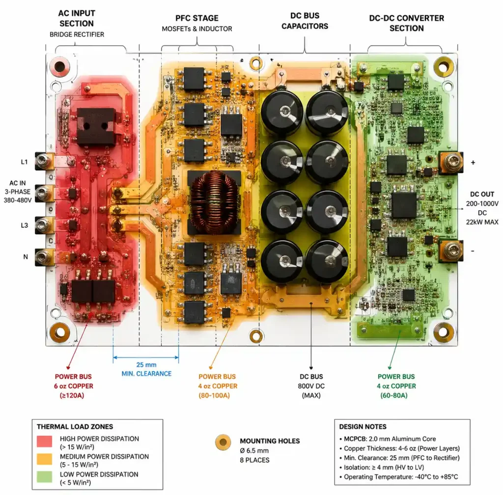
DC-DC Converter Module: Highest power density – switching freqs 50-200 kHz, SiC MOSFETs or GaN HEMTs generating 50-100W in a 10×10mm footprint. Use 4 oz copper minimum, 6.0 W/m·K dielectric if density exceeds 150 W/in². Keep gate traces under 20mm – even on single-layer MCPCB, loop inductance matters.
DC Output Filter and Current Sensing: Lower thermal load but needs EMI filtering. If power switching and filtering share the same MCPCB, use a ground plane under low-signal traces. Shunt resistors for 100-400A sensing should be 6-10 oz copper with Kelvin connection pads. Position these at the board edge where the metal base can couple to an external heatsink if needed.
FAQ
Q: What’s the minimum dielectric breakdown voltage I need for a 400V DC bus?
IPC-2221 calls for 2.5 kV minimum at 400V working voltage. Spec 3.0-4.0 kV for margin against transients and aging. Always request hipot testing at 600V DC during manufacturing – don’t skip this.
Q: Can I use thermal vias on MCPCB to improve heat dissipation?
Thermal vias in the copper layer help spread heat laterally, but drilling through the metal base compromises thermal and mechanical performance. Use them sparingly, keep 5mm edge clearance. If you need extensive via routing, consider hybrid rigid-flex construction instead.
Q: How do I calculate trace width for high current on MCPCB?
Use IPC-2152 nomographs with the “thermal relief” curve – the metal base acts as a heatsink. For 4 oz copper on aluminum MCPCB, 10mm trace handles roughly 80-100A with 30°C temp rise. Always run thermal simulation for critical paths.
Q: Should I use aluminum or copper base for a 150kW DC fast charger?
Aluminum works if you spec high-thermal-conductivity dielectric (6.0-8.0 W/m·K) and proper heatsinking. Copper base is only justified above 200 W/in² power density or when you need to meet automotive reliability (AEC-Q) requirements.
Q: What surface finish for power component pads?
ENIG is the standard – flat, solderable, survives multiple reflow cycles. For pads above 100A, consider hard gold plating or OSP if you’re using press-fit terminals instead of soldering.
Conclusion
For Level 2 chargers, aluminum base with 2.0-3.0 W/m·K dielectric and 2-4 oz copper works. For DC fast chargers above 100kW, step up to 6.0-8.0 W/m·K and 4-6 oz copper. Before sending Gerbers, double-check clearance rules, copper thickness for continuous current, and dielectric breakdown voltage. Get your fabricator involved early – MCPCB panelization and lead times differ from FR4. For related high-power applications, our guide on industrial motor driver PCBs covers similar thermal and current-handling principles.