
HDI PCB Via Types Explained: Blind, Buried, and Microvia Comparison
When designing high-density interconnect (HDI) PCBs, via selection impacts routing density, signal integrity, cost, and reliability. Unlike through-hole vias that penetrate every layer, HDI boards use blind vias, buried vias, and microvias to optimize layer utilization. This guide explains manufacturing processes, design rules, cost factors, and reliability based on production data and IPC standards.
What Are HDI PCB Vias?
HDI vias connect copper layers without consuming routing space on every layer. Through-hole vias drill from top to bottom through all layers. This works for 4-to-8-layer designs but wastes routing channels on high-layer-count boards.
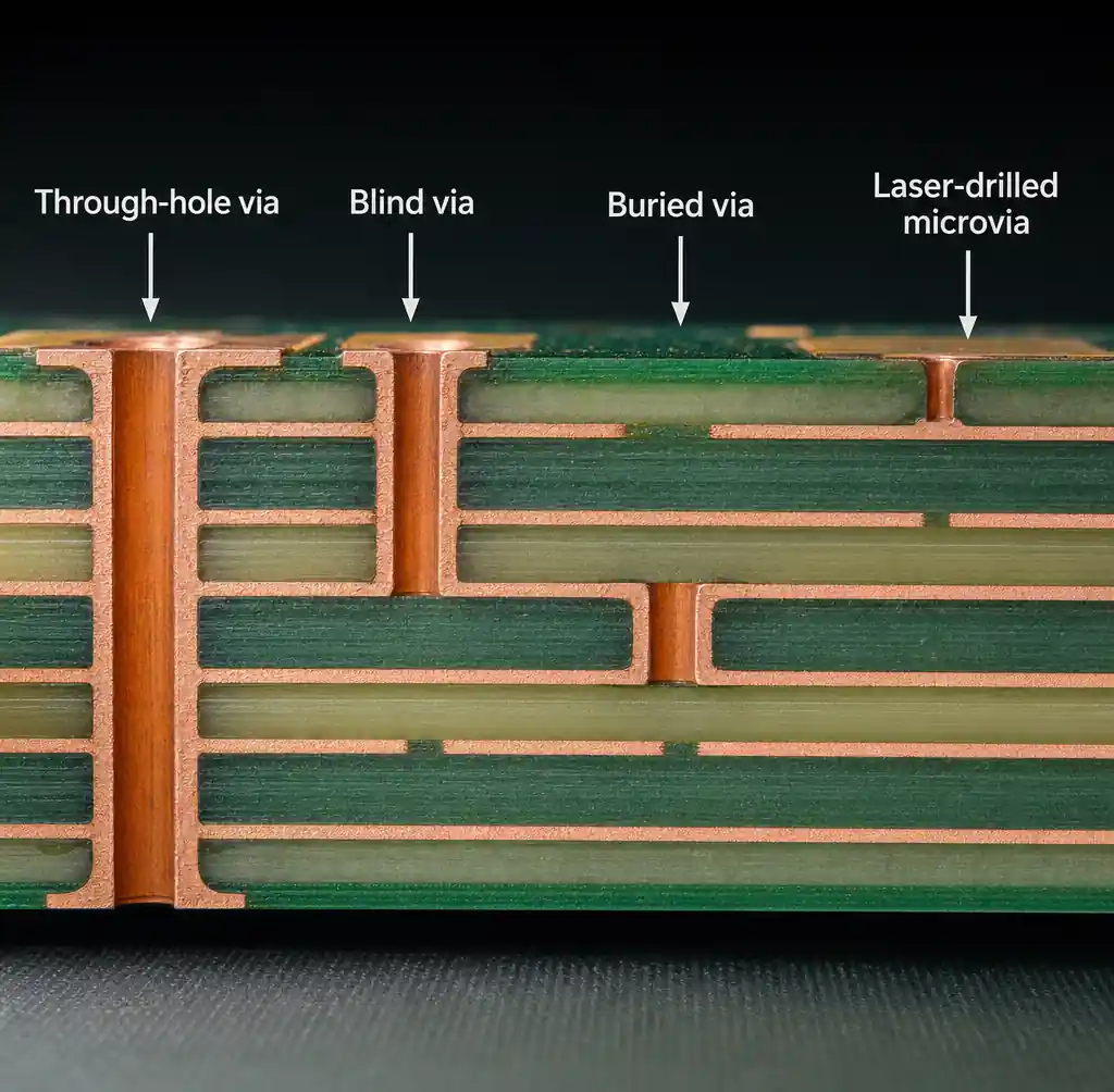
HDI vias connect only the layers needing electrical continuity. Blind vias connect an outer layer to inner layers without reaching the opposite surface. Buried vias connect internal layers exclusively. Microvias use laser drilling to create small-diameter connections (≤150 µm), enabling fine-pitch BGA breakout.
Blind Via: Definition and Manufacturing
Blind vias start at an outer layer and terminate at a specific inner layer. They appear as holes on one surface but don’t penetrate to the opposite side. Manufacturing uses controlled-depth mechanical drilling or laser ablation, followed by electroless copper deposition and plating.
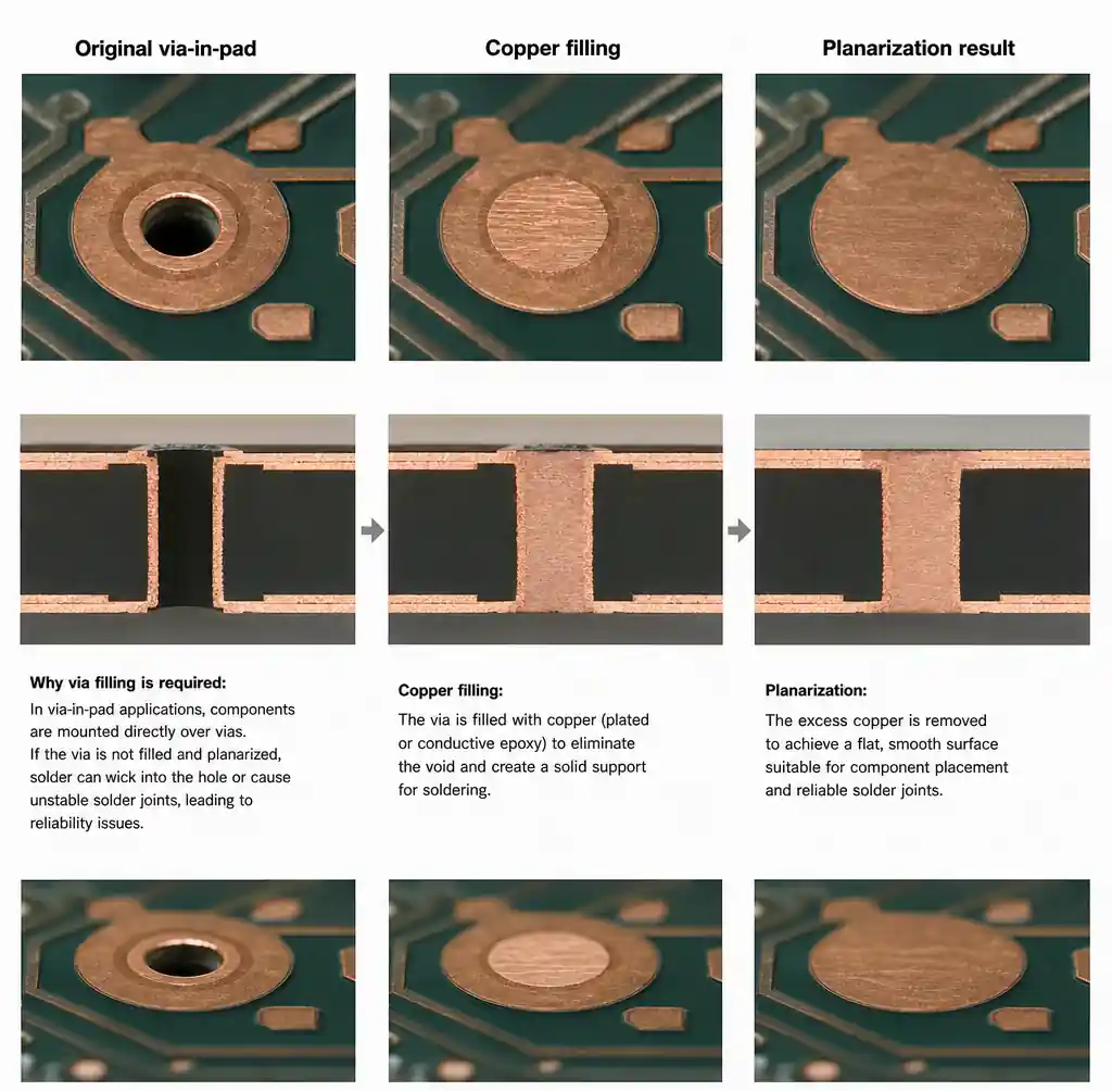
Drilling depth must stop precisely at the target layer—overshooting damages inner plane integrity, undershooting creates open circuits. Most manufacturers use depth-controlled drills for blind vias, with laser drilling for microvias. After plating, vias are filled with epoxy for via-in-pad applications.
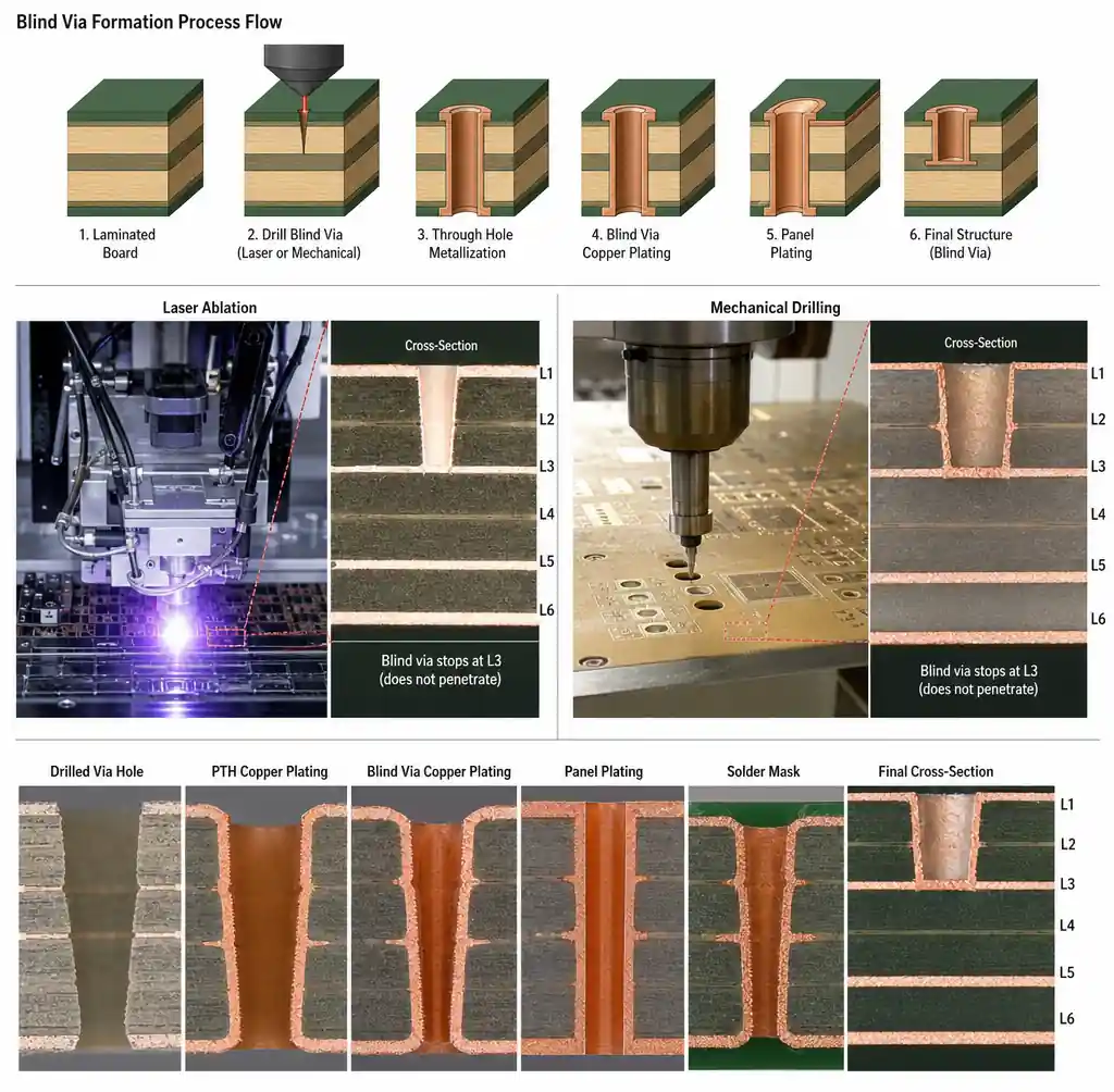
Blind vias enable layer-specific routing without blocking unrelated layers. In an 8-layer board, a blind via connecting L1 to L3 frees routing space on L4 through L8. This becomes critical in HDI boards.
| Blind Via Specification | Typical Value | Design Rule |
|---|---|---|
| Minimum drill diameter | 0.15 mm (laser) / 0.20 mm (mechanical) | Match manufacturer capability |
| Aspect ratio limit | 1:1 (laser) / 8:1 (mechanical) | Depth ÷ diameter |
| Pad size (finished) | Drill + 0.15 mm | Annular ring ≥0.05 mm |
| Cost multiplier | 1.5–2.3× | vs through-hole |
Buried Via: Internal Layer Connections
Buried vias connect only internal layers and are hidden from both surfaces. They require sequential build-up: inner layer pairs are drilled, plated, and laminated before outer layers are added.
Manufacturing steps: fabricate inner core layers, drill and plate buried vias, laminate additional prepreg and copper, then repeat for each build-up layer. Registration accuracy is critical—each lamination cycle must align precisely with formed vias. Misalignment causes open circuits.
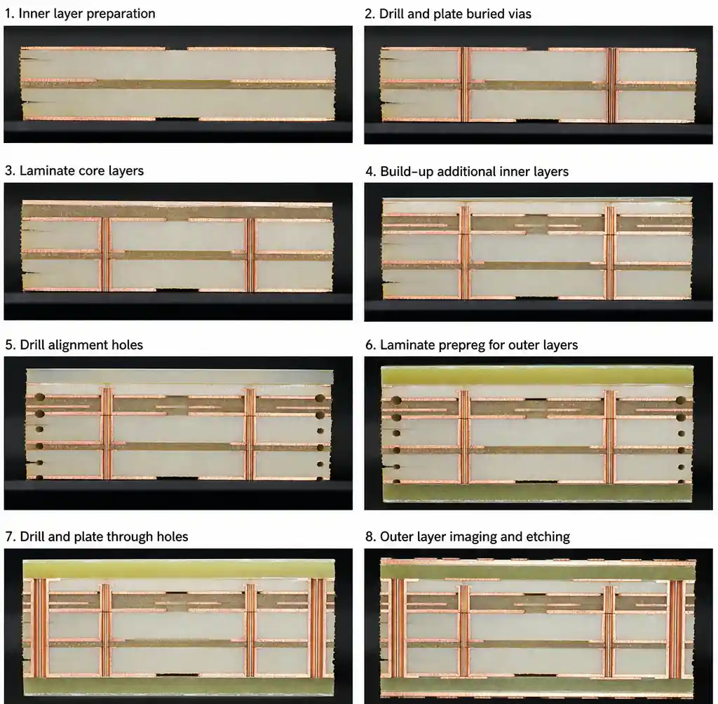
Buried vias provide maximum surface routing freedom. In a 10-layer board with buried vias connecting L4 to L7, both surfaces remain unobstructed. This suits high-pin-count BGAs where escape routing must fan out beneath components.
Cost impact is significant. Each buried via layer pair requires separate drilling, plating, and inspection. Lead time increases 3–5 days versus through-hole designs.
Microvia Formation: Laser Drilling vs Photo Via
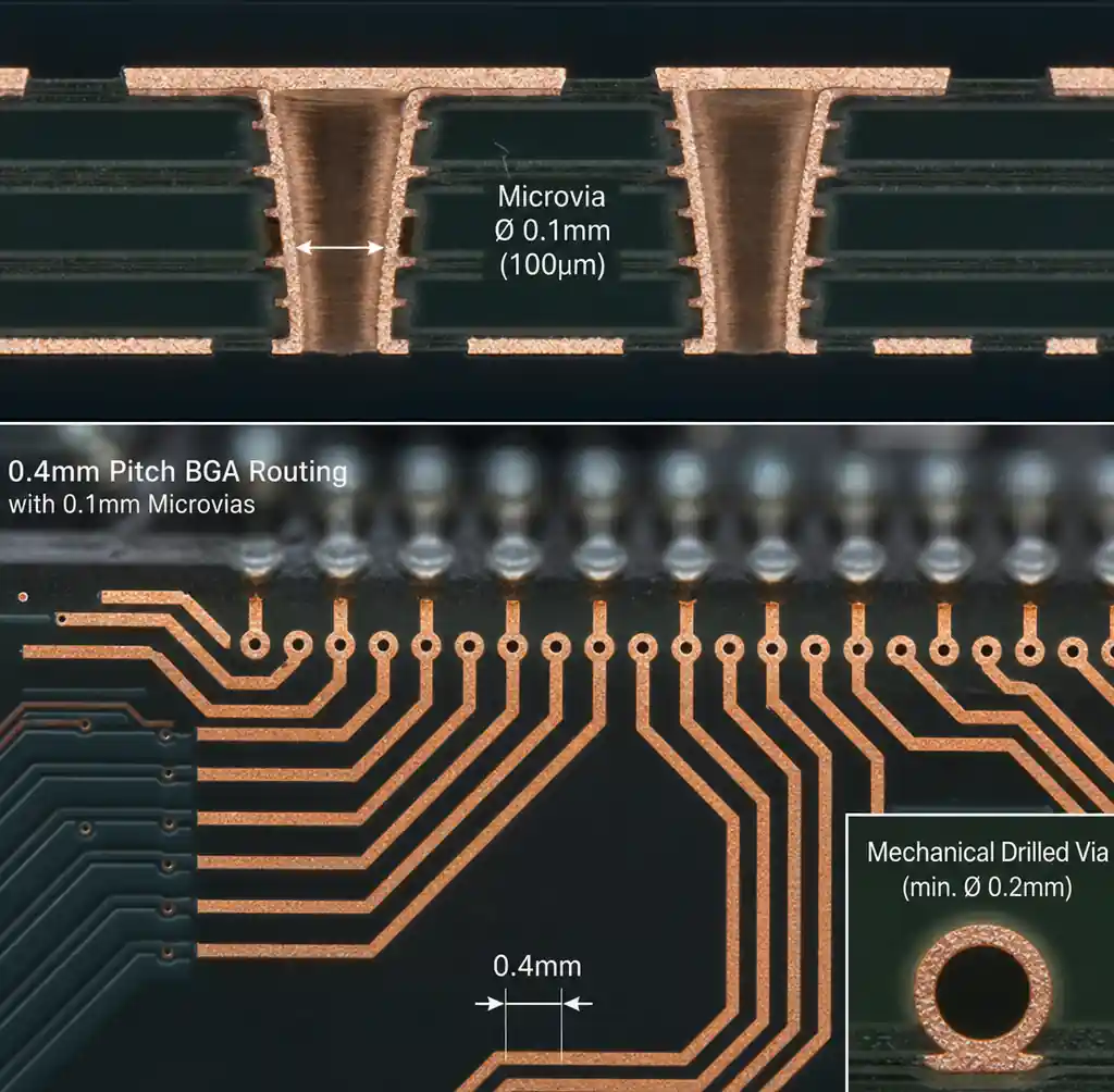
Microvias have diameters ≤150 µm, formed by laser ablation rather than mechanical drilling. The laser removes dielectric to expose underlying copper, creating a tapered profile with 10–15° sidewall angle. This ensures reliable plating coverage.
Two laser methods dominate: CO₂ laser and UV laser. CO₂ lasers vaporize dielectrics like FR-4 efficiently but require a copper stop layer. UV lasers provide finer resolution and drill through thin copper directly. Most HDI manufacturers use CO₂ lasers for throughput and cost.
Photo vias use photoimageable dielectrics. The layer is exposed through a photomask, developed to create openings, then plated. Photo vias enable extremely high density but cost more.
| Microvia Parameter | Laser Drilled | Photo Via |
|---|---|---|
| Minimum diameter | 0.05–0.15 mm | 0.03–0.10 mm |
| Aspect ratio | 0.75:1 | 1:1 |
| Sidewall profile | Tapered (10–15°) | Vertical |
| Cost per 1000 vias | $8–$25 | $15–$40 |
| Throughput | 3000–8000/hr | 1000–3000/hr |
Microvias enable fine-pitch component placement mechanical drilling cannot support. A 0.4 mm pitch BGA requires 0.1 mm microvias—0.2 mm mechanically drilled holes would prevent breakout.
Stacked vs Staggered Microvias
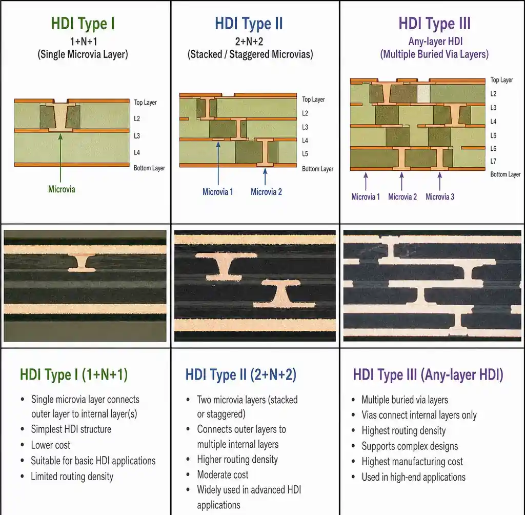
HDI designs often require connections spanning multiple layer pairs. Two configurations address this: stacked and staggered microvias. The choice trades routing density for reliability and cost.
Stacked microvias align vertically through multiple build-up layers, creating direct Z-axis connections. They consume minimal board area and maximize routing density beneath BGAs. However, stacked microvias require copper filling between each lamination cycle. This adds cost and time. The vertical copper column concentrates thermal stress, increasing failure risk.
Staggered microvias offset at each layer, connected by short traces or pads. This distributes mechanical stress along a stepwise path. Staggered microvias eliminate via filling between layers, reducing cost and complexity. Testing shows staggered microvias survive 30–40% more thermal cycles before failure. The trade-off is increased routing area—stagger distance typically ranges 0.2–0.5 mm.
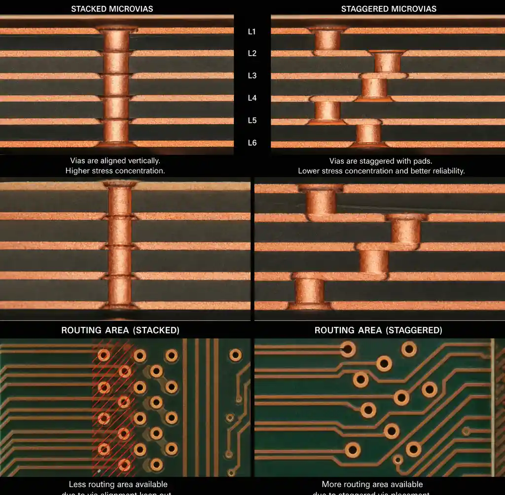
IPC-2226 recommends staggered microvias for Class 3 applications (high reliability) and permits stacked for Class 2 with proper filling. Our automotive PCB data confirms staggered microvias show 12% lower failure rates in IPC-TM-650 thermal cycling tests.
Cost Implications by Via Type
Via selection impacts PCB cost through setup charges, per-via fees, and yield. Understanding cost structure helps optimize designs.
Through-hole vias set the baseline: $15–$50 per panel setup plus $0.002–$0.008 per hole. An 8-layer board with 500 through-hole vias adds $55–$90 per panel.
Blind vias increase costs 1.5–2.3× versus through-hole. The premium comes from controlled-depth drilling, additional plating, and via filling when required. Laser-drilled blind microvias cost $80–$250 per panel setup plus $0.008–$0.025 per via.
Buried vias carry highest cost impact due to sequential lamination. Each buried via layer pair adds 3–5 days and 25–40% to board cost. A 10-layer HDI board with two buried via pairs typically costs $350–$600 in prototypes.
| Via Type | Setup Cost/Panel | Per-Via Cost | Lead Time Impact |
|---|---|---|---|
| Through-hole | $15–$50 | $0.002–$0.008 | Baseline |
| Blind via | $80–$250 | $0.008–$0.025 | +2–3 days |
| Buried via | $150–$400 | $0.015–$0.040 | +3–5 days |
| Stacked microvia | $200–$500 | $0.020–$0.050 | +4–7 days |
Component placement over vias (via-in-pad) requires filling and planarization, adding 15–25% cost but reducing board area by 20–30%. For cost-sensitive designs, limit HDI vias to critical areas.
Design Rules for Each Via Type
Reliable HDI via design requires adherence to manufacturer capabilities and IPC specifications.
Blind via rules:
- Minimum annular ring: 0.05 mm (IPC-6012 Class 2), 0.075 mm (Class 3)
- Aspect ratio: ≤1:1 for laser microvias, ≤8:1 for mechanical
- Clearance: ≥0.10 mm (Class 2), ≥0.15 mm (Class 3)
- Via-in-pad fill required for component mounting
Buried via rules:
- Registration tolerance: ±0.05 mm between lamination cycles
- Minimum capture pad: drill diameter + 0.20 mm
- Aspect ratio: ≤8:1
- Board edge clearance: ≥1.0 mm
Microvia rules:
- Single-layer span only
- Minimum land diameter: 0.20–0.30 mm
- Stacked: maximum 2–3 levels with copper filling
- Staggered: offset ≥0.25 mm between levels
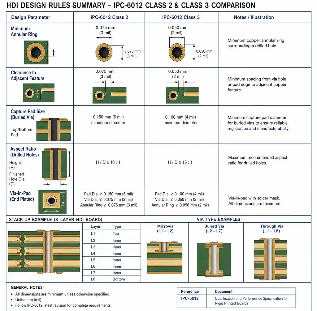
Always consult your manufacturer’s capability table before finalizing via specs. Capabilities vary between shops.
Reliability Comparison: Thermal Cycling Performance
HDI via reliability depends on plating quality, thermal expansion mismatch, and mechanical stress distribution. IPC-TM-650 Method 2.6.27A defines thermal stress testing where coupons undergo six reflow cycles at 260°C peak while resistance is monitored. Acceptable performance requires ≤5% resistance increase.
Our 1000-cycle thermal cycling data (-55°C to +125°C per IPC-TM-650 2.6.7) shows clear differences:
- Through-hole vias: <2% failure rate (baseline)
- Blind vias (mechanical): 3–5% failure rate
- Blind microvias (laser, 0.15 mm): 8–12% failure rate
- Buried vias: 4–7% failure rate
- Stacked microvias (2 levels): 15–18% failure rate
- Staggered microvias (2 levels): 10–13% failure rate
Higher microvia failure rates stem from thinner copper plating (12–18 µm vs 25 µm for mechanical vias) and concentrated thermal stress at the via barrel-to-pad interface. Stacked microvias show elevated risk due to vertical stress through multiple interfaces.
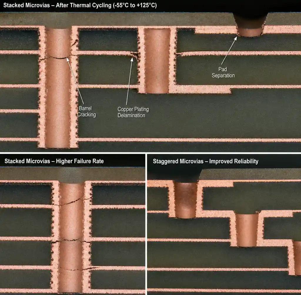
Mitigation strategies: specify thicker copper plating for critical vias (18 µm minimum), use staggered configurations for high-reliability applications, implement copper via filling, and route redundant connections for critical nets.
For medical device PCBs and automotive applications, specify IPC-6012 Class 3 and conduct qualification testing per IPC-TM-650 before production.
FAQ
Q: Can I mix through-hole vias and microvias on the same PCB?
Yes, hybrid stackups using through-hole vias for power/ground and microvias for dense signal routing are common. This optimizes cost while achieving required density.
Q: What is the minimum microvia diameter manufacturers can produce?
Most PCB manufacturers offer 0.10–0.15 mm laser-drilled microvias as standard. Advanced shops achieve 0.05–0.08 mm, but yield drops and cost increases. Verify capability before specifying ultra-small vias.
Q: How many microvia levels can I stack?
IPC-2226 permits up to 3 stacked levels with proper copper filling. Most manufacturers recommend maximum 2 levels for reliability. Beyond 2 levels, consider any-layer HDI or staggered configurations.
Q: Do blind vias require filling?
Filling is optional for standard blind vias but required for via-in-pad where components mount directly over the via. Non-filled vias must have solder mask coverage to prevent wicking during assembly.
Q: What causes microvia reliability failures?
Primary failure modes: insufficient copper plating (<12 µm), inadequate via filling in stacked configurations, registration misalignment between lamination cycles, and thermal expansion mismatch. IPC-TM-650 thermal cycling identifies these before production.
Q: How do I choose between stacked and staggered microvias?
Choose stacked for maximum density when board space is critical and reliability permits (consumer electronics). Choose staggered for high reliability and extended life (automotive, medical, industrial).
Conclusion
HDI PCB via selection balances routing density, cost, and reliability. Through-hole vias remain cost-effective for standard boards, while blind vias optimize layer utilization. Buried vias provide maximum surface routing freedom at significant cost. Microvias enable fine-pitch BGA breakout essential for miniaturized electronics.
Manufacturing method drives performance: mechanical drilling offers proven reliability and lower cost, while laser drilling enables ultra-small diameters for advanced packaging. Staggered microvia configurations improve thermal cycling reliability by 30–40% versus stacked designs but consume more area.
Design decisions must align with application requirements. Cost-sensitive products benefit from Type I HDI with single-level microvias. High-reliability applications justify staggered configurations and IPC-6012 Class 3 specs. Validate via design rules against manufacturer capabilities and conduct IPC-TM-650 qualification testing for mission-critical products.
At Andwin Circuits, we manufacture HDI PCBs from Type I through Type III with laser-drilled microvias down to 0.10 mm. Our HDI capabilities include stacked and staggered configurations, blind and buried vias, and via-in-pad processing. Contact us to discuss your HDI design requirements.