
BGA PCB Design Guidelines: Escape Routing and Via Optimization
Modern BGA packages now exceed 2000 balls with pitches as tight as 0.3mm, creating routing densities that push traditional PCB design to its limits. When Texas Instruments analyzed field failures in automotive processors, 34% of signal integrity issues traced back to improper BGA fanout design and via placement—failures that manifested only after thermal cycling revealed latent impedance mismatches.
If you want to design reliable BGA layouts for high-pin-count processors, FPGAs, or power management ICs, you must understand escape routing strategies, via optimization techniques, HDI stackup requirements, and thermal management. This guide provides practical design rules based on production data from thousands of BGA designs.
What Is BGA Escape Routing?
BGA escape routing refers to the technique of routing signal traces from ball grid array pads to vias or routing channels on other layers. The fundamental challenge is extracting hundreds or thousands of signals from a dense ball field without creating routing congestion, impedance discontinuities, or thermal bottlenecks.
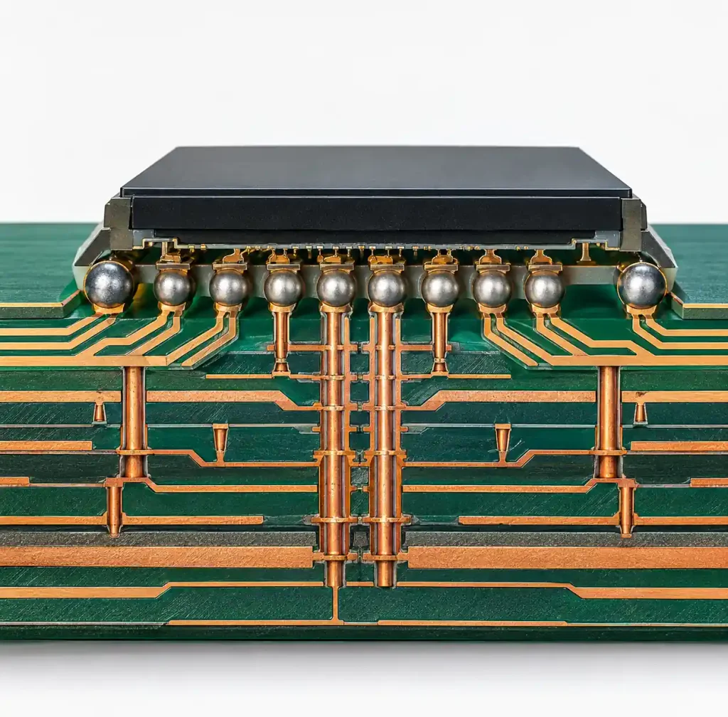
For a 0.8mm pitch BGA with 324 balls, outer row balls can escape using dog-bone routing with adjacent vias. However, inner balls require layer transitions through blind vias, buried vias, or via-in-pad structures. A 0.4mm pitch BGA with 900 balls demands HDI technology with microvias—conventional PCB processes cannot achieve the required routing density.
According to IPC-7351 land pattern standards, BGA pad dimensions depend on ball diameter and density level. For 0.5mm pitch with 0.3mm balls, NSMD (non-solder mask defined) pads typically measure 0.25-0.28mm diameter. The escape routing strategy must work within these pad dimensions while maintaining controlled impedance for high-speed signals.
BGA Pitch and Escape Routing Strategy Selection
BGA ball pitch directly determines which escape routing techniques are feasible and which HDI technologies you need. The pitch represents the center-to-center spacing between adjacent balls, ranging from 1.27mm down to 0.3mm in ultra-high-density mobile processors.
| BGA Pitch | Escape Strategy | Via Technology | Trace/Space | HDI Required |
|---|---|---|---|---|
| 1.0-1.27mm | Dog-bone fanout | Through-hole vias | 6/6 mil | No |
| 0.8mm | Dog-bone outer, via-in-pad inner | Mechanical blind vias | 5/5 mil | Optional |
| 0.5mm | Via-in-pad required | Laser microvias | 3/3 mil | Yes |
| 0.4mm | Via-in-pad + stacked microvias | Laser microvias | 3/3 mil | Yes |
| 0.3mm | Via-in-pad + multiple microvia layers | Stacked laser microvias | 2.5/2.5 mil | Yes |
The transition point between conventional and HDI processes occurs around 0.5-0.65mm pitch. Above 0.8mm pitch, you can use standard FR-4 stackups with through-hole vias. Below 0.5mm pitch, you enter HDI territory requiring sequential lamination, laser-drilled microvias, and significantly tighter manufacturing tolerances.
You should specify via-in-pad when BGA pitch drops below 0.65mm or when routing density demands every available channel. While via-in-pad adds 15-25% to fabrication cost due to filling and planarization requirements, it eliminates dog-bone trace stubs that degrade signal integrity above 5 GHz.
Dog-Bone vs Via-in-Pad Escape Techniques
Dog-bone routing uses a short trace (0.2-0.4mm) from the BGA pad to an adjacent via. This works for coarse-pitch BGAs (0.8mm+) where space accommodates the trace stub and via. Keep dog-bone length under 0.5mm to minimize stub resonance. Design rules: minimum trace length 0.15mm, maximum 0.5mm, stagger via positions between rows, maintain 0.15mm minimum spacing to adjacent pads.

Dog-bone offers cost advantages since vias don’t require filling. However, for signals above 10 GHz, the stub degrades return loss.
Via-in-pad places the via directly within the pad, eliminating the dog-bone trace. This becomes necessary for fine-pitch BGAs (0.5mm and below) where insufficient space exists for dog-bone routing. Via-in-pad improves signal integrity and provides superior thermal dissipation.
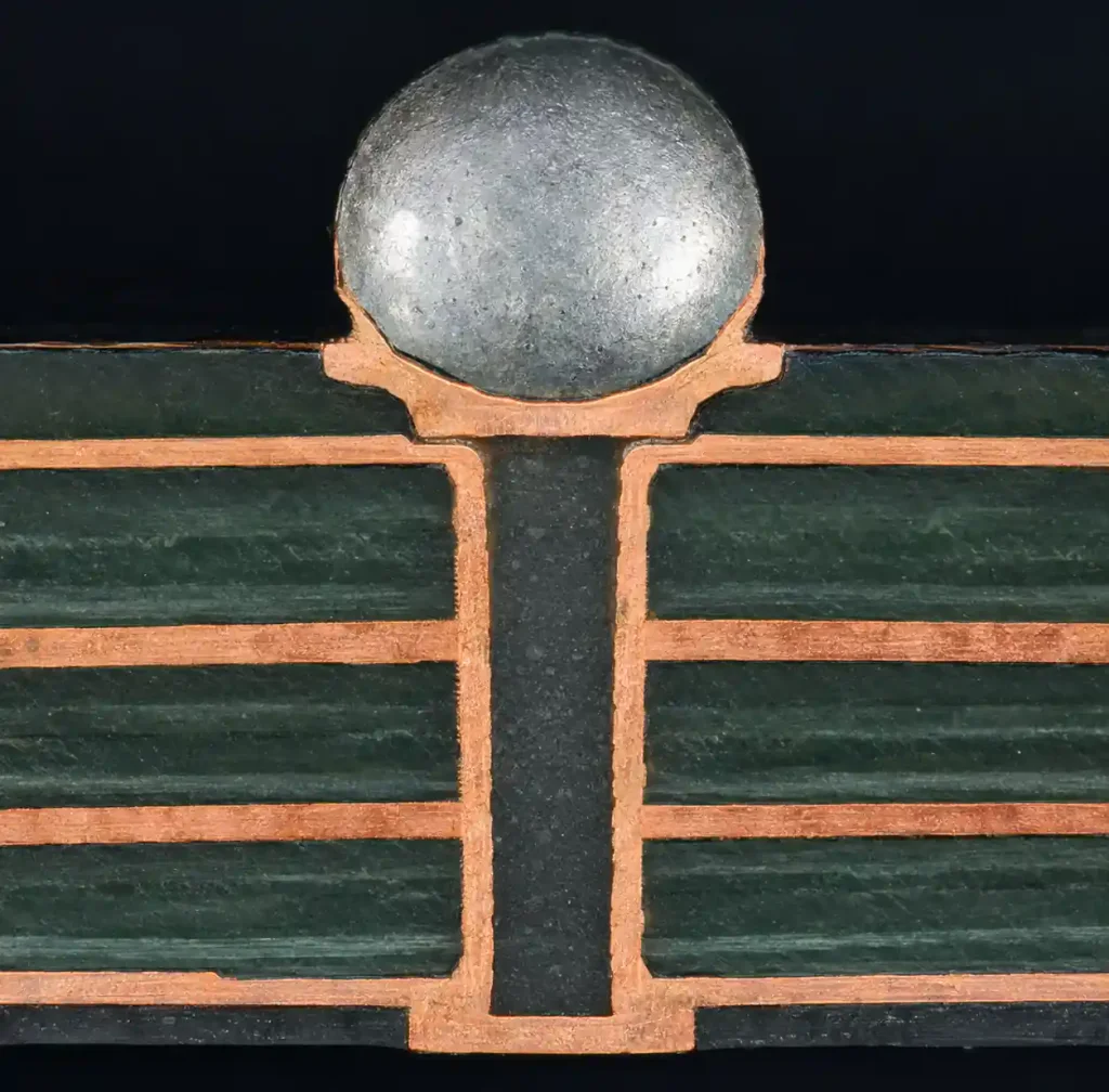
The via must be filled with conductive or non-conductive epoxy to prevent solder wicking. Via-in-pad adds 15-25% to fabrication cost but enables routing densities impossible with dog-bone. A study of 10 Gbps channels showed via-in-pad reduced insertion loss by 0.4-0.6dB at 5 GHz. High-speed differential pairs benefit from via-in-pad even on coarse-pitch BGAs.
HDI Stackup Design for BGA Escape Routing
High-density interconnect (HDI) technology enables BGA escape routing through microvias and blind/buried vias. HDI stackups use sequential lamination to build up layers in stages, creating routing channels for dense ball fields.
Common HDI configurations: 1+N+1 (one build-up layer per side, 8-10 total layers) and 2+N+2 (two build-up layers per side, 12-16 layers). For a 0.5mm pitch BGA with 676 balls, a 10-layer HDI stackup arranges layers as: L1 (signal) – L2 (ground) – L3 (signal) – L4 (ground) – L5-L6 (core) – L7 (ground) – L8 (signal) – L9 (ground) – L10 (signal).
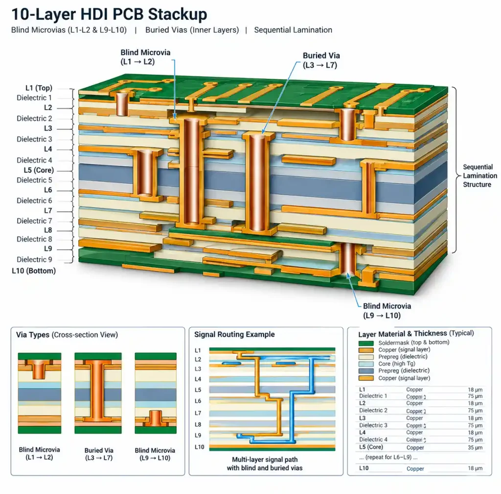
HDI design rules: microvia diameter 0.1-0.15mm laser-drilled, depth single build-up layer (0.05-0.1mm), stacked microvias offset by 0.1mm or use copper-filled construction, 0.05mm minimum annular ring, and 1:1 or lower aspect ratio.
Where conventional 8-layer construction handles 300-ball BGAs at 0.8mm pitch, 10-layer 1+N+1 HDI accommodates 900-ball devices at 0.5mm pitch. Learn more about HDI PCB manufacturing.
Stacked vs Staggered Microvia Design Trade-offs
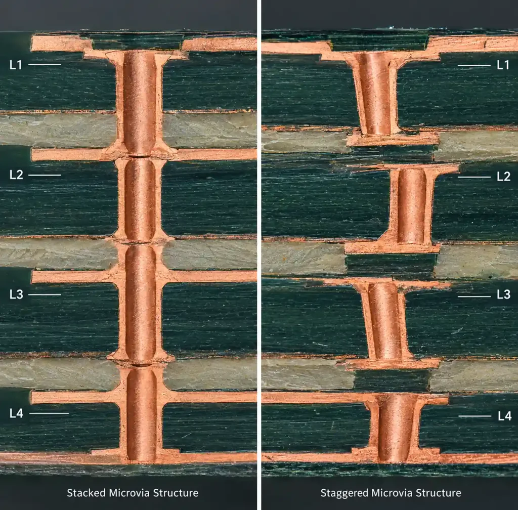
Stacked microvias align vertically through successive layers, while staggered microvias offset laterally between transitions. Stacked preserve routing channels by occupying the same XY location, maximizing routing area but requiring tight registration (±0.025mm). Staggered shift 0.15-0.2mm laterally, providing forgiving tolerances (±0.05mm) but consuming more area.
| Microvia Type | Routing Density | Cost | Tolerance | Best Application |
|---|---|---|---|---|
| Stacked | Saves 40% area | +20-30% | ±0.025mm | 0.4mm pitch and below |
| Staggered | Standard | Baseline | ±0.05mm | 0.5-0.65mm pitch |
Use stacked microvias when pitch is 0.4mm or below. Staggered work better for 0.5-0.65mm pitch. Consider via-in-pad design rules for reliability.
Thermal Pad Design and Via Optimization
Many BGAs include an exposed thermal pad that requires special via design to conduct heat through the PCB. Design parameters: via diameter 0.3-0.4mm, pitch 0.8-1.2mm spacing, quantity 9-25 vias for 3×3mm pad or 25-100 vias for 10×10mm pad, conductive fill provides 3-5× better conductance than non-conductive.
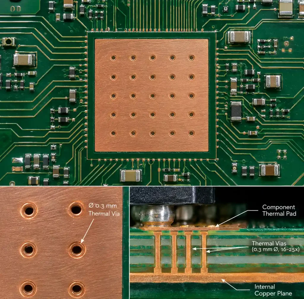
A thermal via array with 16 vias (0.3mm diameter) through 1.6mm board provides ~12-18°C/W thermal resistance. Doubling to 32 vias reduces resistance to 8-12°C/W. Use via-in-pad construction for thermal vias—placing vias outside adds 5-10°C/W resistance. For metal core PCB provides superior performance.
NSMD vs SMD Pad Design for BGA Assembly
BGA pad design affects solder joint reliability. NSMD (non-solder mask defined) pads expose the entire copper pad with solder mask opening 0.05-0.1mm larger than pad. Solder wets both pad top and sidewalls, creating robust connections. SMD pads have solder mask overlapping copper edges, with mask opening smaller than pad.
| Pad Type | Solder Joint Strength | Routing Flexibility | Recommendation |
|---|---|---|---|
| NSMD | Higher (full sidewall wetting) | Better | IPC-7351 preferred |
| SMD | Standard | Limited | Legacy only |
IPC-7351 recommends NSMD with solder mask opening 0.1mm larger than copper pad. For 0.25mm copper pad, specify 0.35mm mask opening. Always use NSMD for fine-pitch BGAs (0.5mm and below). Review PCB assembly inspection standards.
Controlled Impedance Routing from BGA Signals
High-speed BGA signals require controlled impedance routing. USB 3.2, PCIe Gen 4, DDR5 demand tight impedance control through BGA fanout. Optimization techniques: via-in-pad eliminates stub inductance (removes 0.2-0.4nH), back-drilling eliminates via stubs, matched via pad sizes maintain consistent loading (0.4-0.5pF), immediate transition to controlled impedance trace within 0.5mm, ground via placement within 0.5mm of signal via.

For 50Ω single-ended signals on 10-layer HDI with 0.1mm dielectric, use 0.1mm trace width. Differential pairs require tight coupling—route with 2-3× trace width spacing for 100Ω impedance. Target ±10% impedance tolerance through fanout region. Explore controlled impedance PCB design.
FAQ
What is the difference between dog-bone and via-in-pad BGA escape routing?
Dog-bone routing uses a short trace from the BGA pad to an adjacent via, while via-in-pad places the via directly inside the pad. Dog-bone works for coarse-pitch BGAs (0.8mm+) and costs less since vias don’t need filling. Via-in-pad is required for fine-pitch devices (0.5mm and below), saves routing space by 30-40%, and improves signal integrity by eliminating stub inductance.
When do I need HDI technology for BGA designs?
HDI becomes necessary when BGA pitch drops below 0.65mm or when routing density exceeds conventional layer capabilities. A 0.5mm pitch BGA with 500+ balls typically requires 10-layer 1+N+1 HDI construction with laser-drilled microvias. Coarse-pitch BGAs (0.8-1.0mm) can often be routed on standard 8-layer stackups.
How many thermal vias do I need under a BGA thermal pad?
Via count depends on power dissipation. For 2-5W devices, use 16-25 thermal vias (0.3mm diameter). For 5-10W, increase to 36-49 vias. Above 10W, consider metal core PCB or active cooling. Thermal resistance: 16 vias provides ~15°C/W, 36 vias gives ~10°C/W, while 64 vias reaches ~8°C/W.
Should I use stacked or staggered microvias for BGA fanout?
Use stacked microvias when pitch is 0.4mm or below, as they preserve routing channels by occupying the same XY location. Staggered microvias work better for 0.5-0.65mm pitch and provide more forgiving manufacturing tolerances (±0.05mm vs ±0.025mm for stacked). Stacked construction saves 40% routing area but demands qualification testing.
What is the best pad type for fine-pitch BGA assembly?
NSMD (non-solder mask defined) pads are recommended per IPC-7351 standards. The solder mask opening should be 0.1mm larger than the copper pad diameter. NSMD provides better solder joint reliability through full sidewall wetting and accommodates via-in-pad designs. For 0.5mm pitch BGA with 0.25mm pads, specify 0.35mm solder mask openings.
How do I calculate trace width for controlled impedance BGA routing?
Trace width depends on target impedance, dielectric thickness, and material Dk. For 50Ω microstrip on 0.1mm dielectric with FR-4 (Dk=4.2), use 0.1mm trace width. For 100Ω differential pairs, use 0.1mm traces with 0.2-0.3mm spacing. Maintain impedance-matched trace width immediately after via breakout—within 0.5mm—to minimize reflections.
Conclusion
BGA escape routing and via optimization directly determine whether your high-density designs manufacture reliably and perform to specification. The transition from dog-bone to via-in-pad techniques occurs around 0.5mm pitch, where conventional routing cannot fit between pads. HDI stackups with laser-drilled microvias enable fanout from ultra-dense packages exceeding 1000 balls, while proper thermal via design prevents junction temperatures from exceeding ratings in power applications.
If you need HDI PCB manufacturing for fine-pitch BGA designs, Andwin Circuits offers advanced capabilities up to 50 layers with laser-drilled microvias, via-in-pad construction, and controlled impedance routing for high-speed signals. Our fast delivery in 7 days and IPC-6012 Class 3 quality standards ensure your BGA layouts manufacture correctly on the first build.
Contact us today for custom HDI PCB manufacturing with BGA via-in-pad, microvia stackups, and impedance-controlled routing for your electronic device projects.