
Blind Vias vs Buried Vias: HDI PCB Via Technology Comparison
HDI PCB designs account for over 60% of smartphone mainboards and wearable devices in 2026, with blind and buried vias serving as the backbone for high-density routing. Engineers designing compact electronics face a critical decision: which via technology delivers the routing density, signal integrity, and cost efficiency their product requires?
This guide compares blind vias and buried vias across manufacturing processes, cost implications, reliability considerations, and application scenarios. You will learn when to specify each via type, how drilling methods affect performance, and which HDI build-up structure fits your layer count requirements.
What Are Blind Vias and Buried Vias?
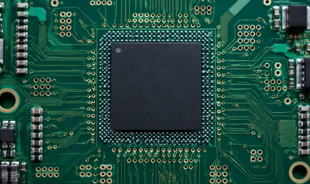
Blind vias connect an outer PCB layer (L1 or L8 in an 8-layer board) to one or more inner layers without penetrating the entire board thickness. A blind via from L1 to L3 leaves layers L4-L8 available for independent routing. This structure enables via-in-pad placements directly under BGA components, saving critical surface area.
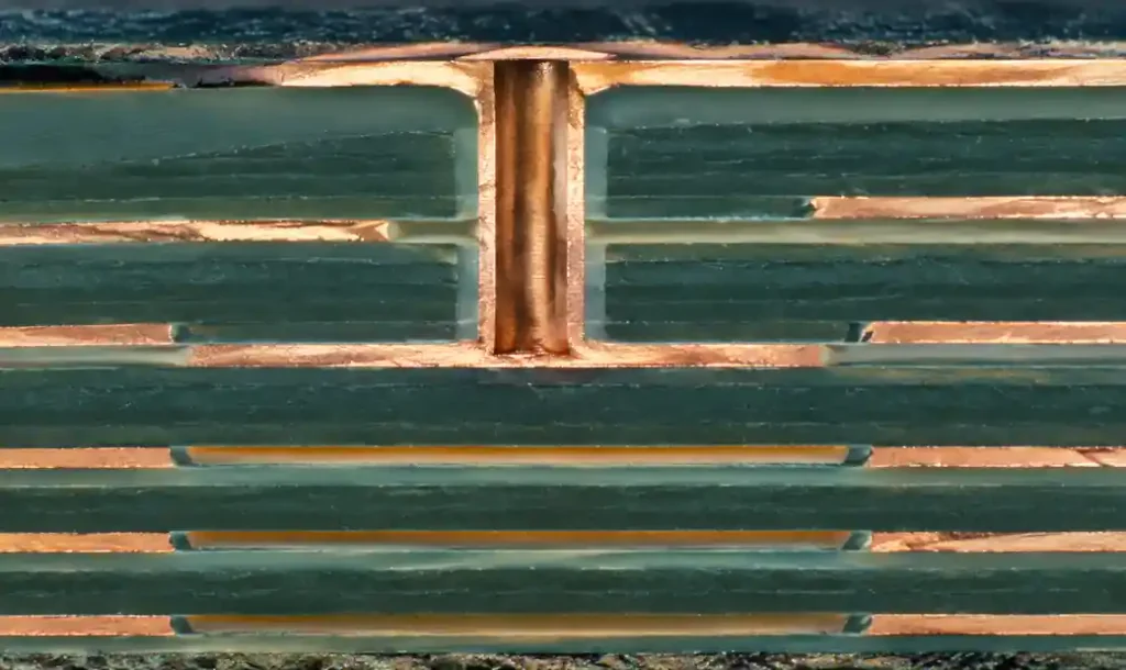
Buried vias connect internal layers exclusively (L3 to L5, for example) and remain invisible from the outer surfaces. Because buried vias do not consume surface real estate, they provide maximum routing flexibility for dense inner-layer nets while preserving outer layers for component placement and high-speed signals.
Both via types reduce board size by 20-35% compared to through-hole vias in multilayer designs above 8 layers, according to IPC-2226 HDI design guidelines. The difference lies in where the connection starts and ends within the PCB stackup.
Manufacturing Process Differences
Blind Via Fabrication
Blind vias use two primary drilling methods: laser drilling for microvias (0.1-0.15mm diameter) and controlled-depth mechanical drilling for larger diameters (0.2-0.4mm). Laser drilling employs CO2 or UV lasers to ablate thin dielectric layers (typically 50-100μm thick) with precision positioning accuracy of ±25μm. The process completes in 0.3-0.8 seconds per via, making it ideal for high-volume production.
Mechanical controlled-depth drilling requires precise z-axis control to stop at the target copper layer without breaking through. Manufacturers monitor drill depth using real-time torque feedback or optical systems. This method handles thicker dielectric stacks (up to 500μm) but operates at slower speeds (2-3 seconds per via) compared to laser systems.

After drilling, blind vias undergo desmear treatment to remove resin residue, followed by electroless copper deposition and panel plating to metallize the via barrel. The plating process typically deposits 18-25μm of copper to ensure reliable electrical connectivity and mechanical strength through thermal cycling per IPC-6012 Class 3 requirements.
Buried Via Fabrication
Buried vias require sequential lamination rather than single-press manufacturing. Fabricators drill and plate vias in the inner-layer core before laminating additional layers on top. For a Type II HDI board with buried vias between L3-L6, the process involves:
- Drill and plate vias in the L3-L6 core subassembly
- Laminate prepreg and copper foil layers L1-L2 and L7-L8 onto the core
- Drill blind vias from outer layers if required
- Complete final plating and surface finish
Each lamination cycle adds 2-3 days to the manufacturing lead time and increases process complexity. The buried vias become permanently embedded within the board structure, making inspection possible only through cross-sectional analysis or X-ray imaging.
Technical Comparison Table
| Parameter | Blind Vias | Buried Vias |
|---|---|---|
| Connection Type | Outer layer to inner layer(s) | Inner layer to inner layer only |
| Visibility | Visible from one surface | Not visible from either surface |
| Drilling Method | Laser or mechanical (controlled depth) | Mechanical before lamination |
| Typical Diameter | 0.1-0.4mm | 0.15-0.5mm |
| Manufacturing Complexity | Moderate (single lamination) | High (sequential lamination) |
| Inspection Method | Visual + AOI + X-ray | X-ray + cross-section only |
| Cost Premium vs PTH | +15-25% for Type I HDI | +40-100% for Type II/III HDI |
Cost Analysis and Layer Count Implications
Blind vias add $28-$85 per board for Type I HDI structures (1+N+1 stackup with blind vias on outer layers only) at prototype volumes of 5-50 pieces. This represents a 15-25% cost increase over standard through-hole PCBs with the same layer count. The premium covers laser drilling equipment time, additional plating cycles, and yield loss from via formation defects.
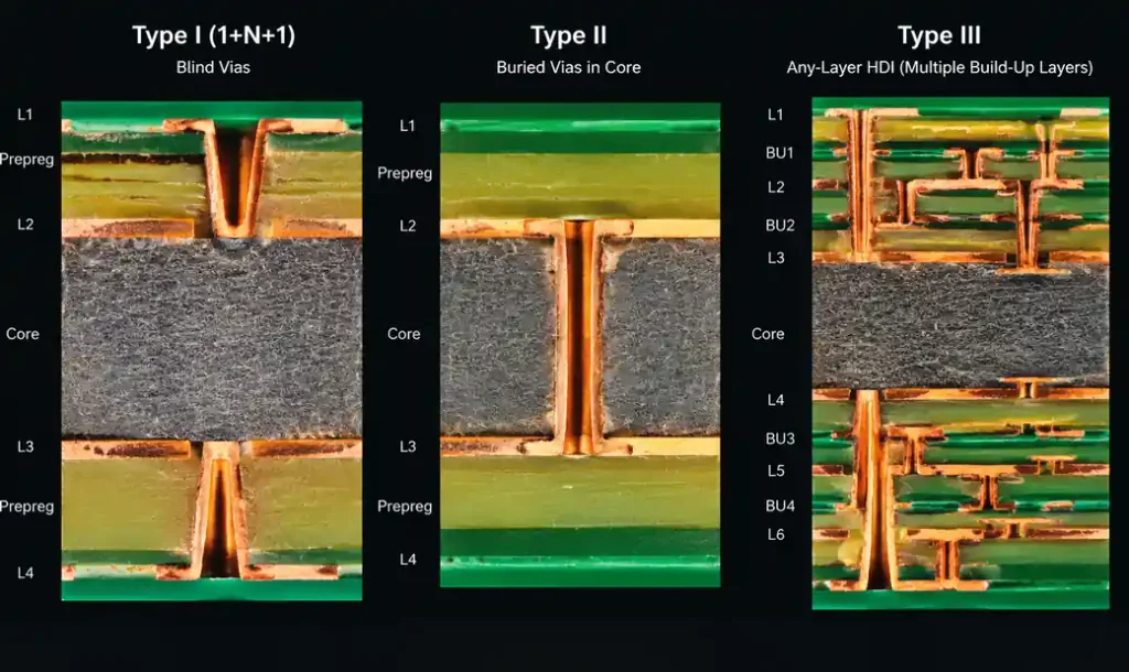
Buried vias escalate costs more significantly because they require sequential build-up processing. Type II HDI boards (1+N+1 with buried vias in the core) typically cost $150-$350 per board at prototype quantities—a 40-100% premium over Type I HDI. Type III HDI designs (2+N+2 or any-layer HDI with stacked microvias) can exceed $500 per board due to multiple lamination cycles and advanced registration requirements.
Layer count directly impacts the cost differential:
- 6-8 layers: Blind vias offer better cost efficiency since routing density gain justifies the premium
- 10-14 layers: Buried vias become economical when inner-layer congestion limits routing options
- 16+ layers: Combined blind and buried vias are often mandatory to achieve required interconnect density
You should calculate the break-even point between adding more layers with through-hole vias versus implementing HDI structures. For products with production volumes above 1,000 units, the board size reduction from HDI often offsets the per-unit cost increase through lower material consumption and improved panel utilization.
Manufacturing Cost Factors Table
| Cost Factor | Blind Vias | Buried Vias | Impact on Total Cost |
|---|---|---|---|
| Drilling Equipment | Laser or precision mechanical | Standard mechanical | +5-10% |
| Lamination Cycles | 1 cycle (standard) | 2-3+ cycles (sequential) | +15-40% |
| Plating Steps | 1 additional plating cycle | 2+ plating cycles | +8-15% |
| Registration Tolerance | ±75μm (standard) | ±50μm (tighter control) | +3-8% |
| Yield Loss Rate | 2-5% defect rate | 5-10% defect rate | +2-10% |
| Inspection Requirements | AOI + X-ray spot check | 100% X-ray + cross-section sampling | +5-12% |
Reliability Considerations
Blind via reliability depends primarily on copper plating quality within the via barrel. Incomplete plating or voids reduce current-carrying capacity and create failure points under thermal stress. IPC-6012 Class 3 specifies minimum 18μm plated copper thickness for HDI microvias, with 25μm preferred for high-reliability applications like automotive and medical devices.
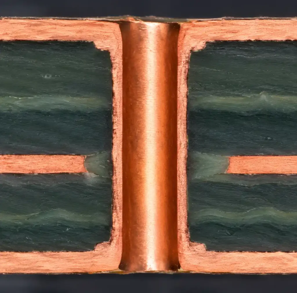
Laser-drilled blind vias exhibit failure rates of 0.5-2% per 1,000 thermal cycles (-40°C to +125°C) when properly designed with adequate land pad sizes and plating thickness. Mechanical-drilled blind vias show slightly higher reliability (0.3-1.5% failure rate) due to smoother via barrel walls that improve copper adhesion.
Buried vias face different reliability challenges:
- Trapped moisture or voids in the laminated dielectric layers
- Coefficient of thermal expansion (CTE) mismatch between core and buildup materials
- Z-axis expansion stress during thermal cycling
- Limited inspectability after lamination
Testing per IPC-TM-650 Method 2.6.8 (thermal stress) demonstrates that buried vias in Type II HDI boards achieve 1,000+ thermal cycles before failure when designed with proper annular ring dimensions (minimum 50μm) and copper thickness specifications. However, the failure mode tends to be catastrophic rather than gradual degradation, making design margin more critical.
Stacked microvias (multiple blind vias aligned vertically) require copper-filled or conductive paste-filled construction to prevent reliability issues. Unfilled stacked vias fail at 200-400 thermal cycles due to stress concentration at the via-to-via interface.
Laser Drilling vs Mechanical Drilling Performance
| Drilling Method | Advantages | Limitations | Best Applications |
|---|---|---|---|
| Laser (CO2/UV) | High speed (0.3-0.8s/via), small diameter (0.1-0.15mm), excellent for thin dielectrics | Limited to single-layer dielectric, aspect ratio <1:1, requires target copper pad | Microvias, Type I HDI, smartphones, wearables |
| Mechanical (Controlled Depth) | Handles multiple layers, larger diameter range (0.2-0.5mm), higher aspect ratio (up to 8:1) | Slower (2-3s/via), drill wear issues, ±25μm depth tolerance | Blind vias spanning 2-4 layers, Type II/III HDI, industrial electronics |
| Plasma Drilling | No drill wear, good for dense via arrays, handles difficult materials | Equipment cost, slower than laser, limited adoption | Advanced HDI, RF applications, ceramic substrates |
Laser drilling achieves superior position accuracy (±25μm) compared to mechanical drilling (±50μm), making it the preferred choice for high-speed PCB designs with controlled impedance requirements. The tighter tolerances reduce stub length variation and improve signal integrity in differential pairs operating above 10 Gbps.
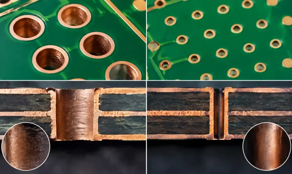
Mechanical drilling provides better via barrel surface quality with less resin smear, reducing desmear process time and improving copper plating adhesion. For buried vias in thick core materials (1.0-1.6mm), mechanical drilling is the only viable option since laser systems cannot ablate through multiple prepreg and copper layers.
HDI Build-Up Structures and Layer Count
Type I HDI (1+N+1): Single buildup layer with blind microvias on each side of a standard core. Suitable for 6-10 layer designs where outer-layer routing density is the primary constraint. Blind vias connect L1 to L2 and L8 to L7 in an 8-layer board, leaving the L3-L6 core available for power planes and inner-layer signals.
Type II HDI (Buried vias + 1+N+1): Adds buried vias within the core layers plus blind vias on outer layers. Required for 10-16 layer designs with high pin-count BGAs (500+ balls) where inner-layer routing congestion prevents signal escape with through-hole vias alone. The buried vias in L3-L6 enable complex power distribution networks and high-speed differential pairs.
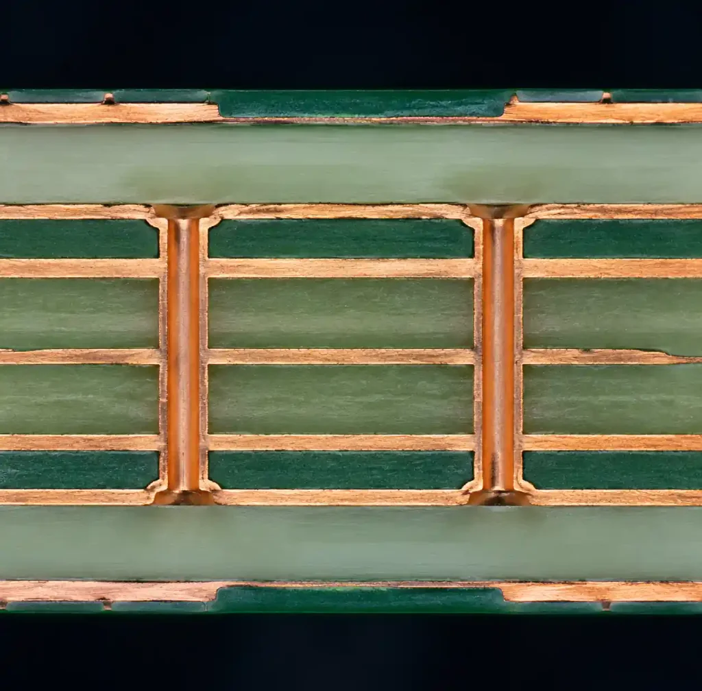
Type III HDI (2+N+2 or Any-Layer): Multiple buildup layers with stacked or staggered microvias connecting any layer combination. Necessary for 16+ layer boards in AI accelerators, 5G infrastructure, and advanced computing applications. A 24-layer any-layer HDI board might use blind vias from L1-L3, L2-L4, buried vias throughout L5-L20, and blind vias from L22-L24, L23-L24 for maximum routing flexibility.
The layer count decision depends on your component density and signal count requirements. Each HDI type has specific cost and manufacturing complexity trade-offs:
- 6-8 layers: Type I HDI with blind vias only (manufacturing lead time +2-3 days vs standard PCB)
- 10-14 layers: Type II HDI with selective buried vias (+5-7 days lead time)
- 16+ layers: Type III HDI or any-layer required (+10-14 days lead time)
When to Use Each Via Type
Specify blind vias when:
- Component density on outer layers requires via-in-pad construction for BGA escape routing
- Board space constraints demand maximum surface area utilization
- You need to reduce EMI by shortening signal return paths between outer and adjacent layers
- Design uses Type I HDI stackup with single buildup layers
- Signal integrity requirements demand reduced via stub length for high-speed signals (>5 Gbps)
Choose buried vias when:
- Inner-layer routing congestion prevents signal completion with through-hole vias
- Power distribution network requires complex connections between internal planes
- Product reliability standards prohibit via-in-pad without plugging (adds cost)
- Design includes 12+ layers with Type II or Type III HDI requirements
- You want to reserve both outer layers exclusively for components and surface routing
Combine both via types when:
- Layer count exceeds 14 layers
- Design includes high pin-count processors (1000+ balls) or FPGAs requiring escape routing from inner rows
- Signal requirements include both high-speed differential pairs (outer layers) and dense power distribution (inner layers)
- Product targets advanced applications like AI servers, 5G base stations, or automotive ADAS systems
The decision should factor in production volume—blind via cost premium becomes negligible above 5,000 units while buried via complexity remains a fixed manufacturing constraint regardless of quantity.
Design Rules and Standards
IPC-2226 provides comprehensive guidelines for HDI PCB design including blind and buried via specifications. Key design rules include:
Minimum annular ring: 50μm for Class 2 (consumer), 75μm for Class 3 (high reliability)
Via aspect ratio limits:
- Laser-drilled blind vias: maximum 1:1 (0.1mm diameter through 0.1mm dielectric)
- Mechanical-drilled blind vias: maximum 8:1 (0.25mm diameter through 2.0mm depth)
- Buried vias: maximum 10:1 depending on drilling capability
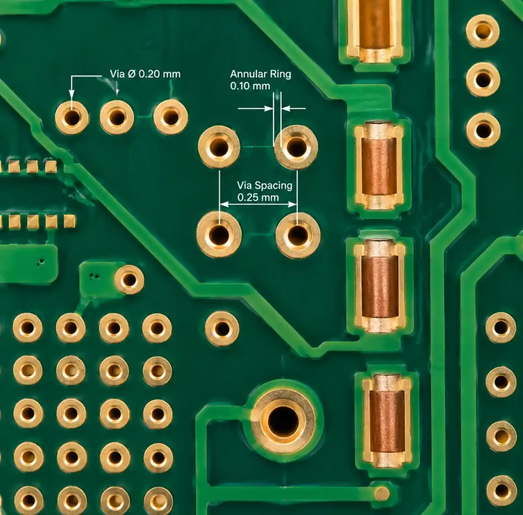
Minimum via-to-via spacing: 0.15mm for laser microvias, 0.25mm for mechanical blind vias
Target pad requirements: Laser-drilled blind vias require copper target pad on inner layer (minimum 0.2mm diameter) for drilling registration and via formation
Andwin Circuits manufactures HDI PCBs with blind and buried vias up to 50 layers, supporting Type I, Type II, and Type III HDI structures. Our facility uses advanced laser drilling systems with ±15μm position accuracy and automated optical inspection to verify via formation quality per IPC-A-600 Class 3 standards.
FAQ
Q: What is the main difference between blind vias and buried vias?
A: Blind vias connect an outer layer to one or more inner layers and are visible from one surface. Buried vias connect only internal layers and are not visible from either board surface. This structural difference affects routing flexibility, cost, and manufacturing complexity.
Q: Are laser-drilled blind vias more reliable than mechanically drilled vias?
A: Both methods achieve comparable reliability when properly designed and manufactured. Laser-drilled microvias show 0.5-2% failure rates per 1,000 thermal cycles, while mechanical blind vias exhibit 0.3-1.5% failure rates. The difference is marginal for most applications. Reliability depends more on plating quality and design margin than drilling method.
Q: How much do buried vias increase PCB cost?
A: Buried vias add 40-100% cost premium for Type II HDI boards at prototype volumes (5-50 units) compared to standard multilayer PCBs. The increase comes from sequential lamination requiring 2-3 build cycles instead of single-press manufacturing. Production volumes above 1,000 units reduce the per-unit premium to 25-40%.
Q: Can I use blind vias for high-speed signals above 10 Gbps?
A: Yes, blind vias improve high-speed signal integrity by reducing stub length compared to through-hole vias. Laser-drilled blind vias with controlled impedance and proper back-drilling or buried via design are standard practice for PCIe Gen 4/5, USB 4.0, and 100G Ethernet applications. Ensure via diameter and pad geometry meet impedance requirements per your signal integrity analysis.
Q: What layer count requires buried vias?
A: Buried vias become necessary at 10-12 layers when inner-layer routing density prevents signal escape with through-hole or blind vias alone. Designs below 10 layers typically achieve adequate routing with Type I HDI (blind vias only). Boards with 16+ layers almost always require both blind and buried vias in Type III any-layer HDI stackups.
Q: How do I inspect buried vias after manufacturing?
A: Buried vias require X-ray inspection since they are not visible from outer surfaces. Manufacturers use automated X-ray inspection (AXI) systems to verify via formation and check for voids or plating defects. Cross-sectional analysis on sample boards provides detailed via barrel and plating quality verification per IPC-6012 requirements.
Conclusion
Blind vias and buried vias serve different purposes in HDI PCB design. Blind vias optimize outer-layer routing density and enable via-in-pad construction for compact BGA escape routing, adding 15-25% cost premium. Buried vias solve inner-layer routing congestion and preserve surface real estate but require sequential lamination that increases cost by 40-100% at prototype volumes.
Your via selection depends on layer count, component density, and signal requirements. Designs with 6-10 layers benefit from blind vias alone (Type I HDI), while 10-14 layer boards often need buried vias in the core (Type II HDI). Boards with 16+ layers typically require both via types in any-layer HDI structures. Laser drilling provides faster processing for thin-dielectric microvias, while mechanical controlled-depth drilling handles multi-layer blind vias. Both methods deliver comparable reliability when manufactured per IPC-6012 Class 3 standards.
Andwin Circuits manufactures HDI PCBs with blind and buried vias up to 50 layers, supporting complex any-layer HDI stackups for advanced electronics applications. Our facility is certified to ISO 9001, IATF 16949, and UL standards, with fast turnaround in 7 days for prototype HDI boards. We have delivered blind and buried via PCBs for automotive ADAS systems, medical devices, 5G infrastructure, and AI computing platforms worldwide.
Contact us today for custom HDI PCB solutions with blind vias, buried vias, or combined any-layer structures. Our engineering team provides stackup design consultation, DFM analysis, and competitive factory-direct pricing.
Word count: 1,799