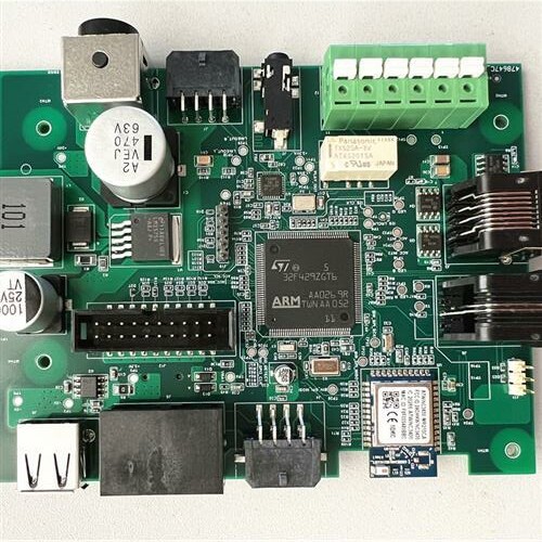
Copy PCB: pcb fab and assembly,pcb assembly manufacturer
In the research of PCB reverse technology,
the reverse push schematic diagram refers to the reverse drawing of the PCB file or the PCB circuit diagram based on the physical product,
which is intended to explain the principle and working condition of the circuit board.
Moreover, this circuit diagram is also used to analyze the functional characteristics of the product itself. In the forward design,
the general product development must first carry out the schematic design,
and then carry out the PCB design according to the schematic.
Whether used to analyze board principles and product operating characteristics in reverse studies,
or to be reused as the basis and basis for PCB design in forward design,
PCB schematics have a special role.
Then, according to the document map or the real thing, how to reverse the PCB schematic diagram,
the reverse push process should pay attention to those details?
1, a reasonable division of functional areas
When the reverse design of the schematic of a good PCB board for pcb fab and assembly,
the reasonable division of functional areas can help engineers reduce unnecessary troubles and improve the efficiency of drawing.
In general, components with the same function on a PCB will be arranged in a centralized manner,
and the functional division area can have a convenient and accurate basis when deducing the schematic.
However, the division of this functional area is not arbitrary.
It requires engineers to have a certain understanding of electronic circuit related knowledge.
First, find out the core components in a functional unit,
and then find out the other components of the same functional unit according to the connection of the traces to form a functional partition.
The formation of functional partitions is the basis for schematic drawing.
In addition, in the process, don’t forget to use the component serial numbers on the PCB board,
they can help you to partition the function faster.
2, find the reference piece
This reference piece can also be said to be the main component of the PCB copying at the beginning of the schematic drawing.
After determining the reference part, drawing according to the pins of these reference parts can ensure the accuracy of the schematic to a greater extent. Sex. For the engineer, the determination of the reference part is not a very complicated matter and pcb assembly manufacturer.
In general, the components that play a major role in the circuit can be selected as the reference parts. They are generally bulky and have many pins, which are convenient for drawing. Such as integrated circuits, transformers, transistors, etc., can be used as a suitable reference.
3, correctly distinguish the line, draw the wiring reasonably
For the distinction between ground, power, and signal lines, engineers also need to have relevant power knowledge,
circuit connection knowledge, PCB wiring knowledge, and so on.
The distinction between these lines can be analyzed from the connection of components,
the width of the copper foil of the circuit, and the characteristics of the electronic product itself.
In the wiring drawing, in order to avoid line crossing and interspersing,
the grounding line can be used in a large number of grounding symbols.
Various lines can be clearly distinguished by using different lines of different colors,
and special signs can be used for various components, and even The unit circuits are drawn separately and finally combined.
4, master the basic framework, draw on similar schematics
For the framework of some basic electronic circuits and the principle drawing method,
engineers need to master, not only to directly draw the basic composition of some simple and classic unit circuits,
but also to form the overall framework of electronic circuits.
On the other hand, don’t neglect that the same type of electronic products have certain similarity in the schematic diagram of PCB copy board and pcb assembly manufacturer.
Engineers can use the same circuit diagram to
carry out the reverse of the new product schematic diagram based on the accumulation of experience.
5. Checking and optimizing
After the schematic drawing is completed, it is necessary to pass the test and check link to conclude the reverse design of the PCB schematic.
The nominal value of the component sensitive to the PCB distribution parameters needs to be checked and optimized.
According to the PCB file diagram, pcb assembly manufacturer, the schematic diagram is compared and analyzed to ensure that the schematic diagram and the file diagram are completely consistent.
If it is found in the check that the schematic layout does not match the requirements,
the schematic adjustment will be carried out until it is completely reasonable and standardized, accurate and clear.
