A Beginner’s Guide to Avoiding PCB Design Mistakes
When beginning PCB design, it’s common to think of the process as simply “connecting the dots”: as long as the connections are made, how those connections are made isn’t particularly important.
Unfortunately, this couldn’t be further from the truth. As PCB design engineers, especially as the speed of electronic devices continues to increase and emissions standards become more stringent, we need to pay attention to the most intricate details of the PCB and our interconnects. If we’re not careful, we can run the risk of poor signal integrity and electromagnetic compatibility.
Having reviewed many other PCB design engineers’ PCBs over the past few years, and looking back at some of my first PC board designs, many of these are common, and unfortunately, mistakes that occur.
This article aims to illustrate the top five beginner PCB design mistakes and what we can do to avoid them. Let’s get started!
1.Trace Spacing

The manufacturer will have a minimum clearance that they can manufacture. The smaller the required clearance, the more the board will generally cost.
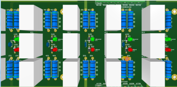
A common beginner mistake is to assume that simply sticking to the minimum allowable or manufacturable clearance is the way to go. As shown above, traces of all signal types are packed together, limited only by the design rules, i.e. the minimum trace spacing allowed by the manufacturer.
Unfortunately, not only is this more difficult to manufacture and prone to lower PCB yields, but this routing style significantly increases coupling between traces, leading to increased crosstalk and noise.
In particular, long, closely spaced, parallel-running traces should not be used unless they cannot be avoided.
Therefore, our first simple tip is to leave ample spacing between traces. As a rule of thumb, this is at least three times the spacing between a signal layer and the adjacent reference layer. For example, with a dielectric thickness of 0.11mm, we want a minimum trace spacing of 0.33mm – but preferably more.
2.Trace Width

Another common beginner PCB design mistake is to use the same trace width for any type of trace. This could be live traces, high impedance nodes, high-speed signals, and so on.
Using the same trace width throughout the design may be convenient, but it is certainly not optimal.
Traces and their widths should be sized based on a variety of factors. For example, traces carrying larger currents should be wider, high impedance and sensitive signal traces need to be thinner, and traces for RF signals often need controlled impedance.
Many people would be surprised to learn, for example, that a 0.2mm wide trace can handle up to about 1 amp of current with only a 20 degree Celsius temperature rise!
Via-Drill Ratio
As was the case with traces, vias also need to be sized appropriately. For vias, we have two main parameters to determine. The total via diameter and the drill diameter. Subtract the drill from the via diameter and halve the result to get the annular ring.
Manufacturers have minimal control over drill diameter and annular ring. Beginner PCB designers often make the drill diameter too large or too small, or the annular ring too small to be reliably manufactured (if at all!).
My recommendation for a “standard” via is a 0.7mm diameter and a 0.3mm drill. Such a via can easily carry about one to two amps of current.
Decoupling
Proper decoupling is an often overlooked aspect for novice PCB design engineers. Unfortunately, however, decoupling is critical to a well-behaved and functioning system.
Good decoupling with low impedance connections ensures that power is properly delivered to ICs that require a lot of energy in a short period of time. This becomes a more critical issue as IC rise and fall times decrease, and current demands increase.
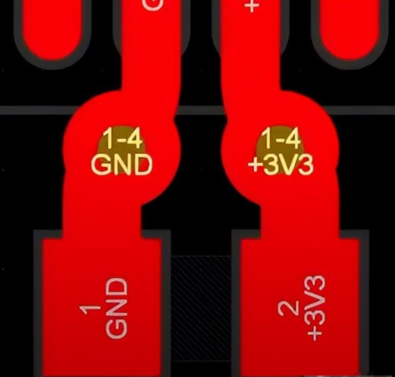
Good decoupling can be achieved by placing decoupling capacitors close to the relevant IC pins, using short and wide traces, and placing power vias close to each other.
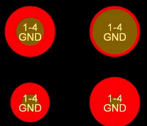
Reference Planes
The last tip is to use a reliable reference (most commonly the “GND” or “0V” plane) in your design.
A large number of design engineers are only concerned with the forward path of the signal. However, signals and power travel in a closed loop and need to return to the source.
It turns out that when an AC (frequency greater than a few kHz) trace is laid out on a PCB, the return current is momentarily in the plane below. This is due to the electromagnetic field that contains the actual energy of the signal and is generated between the trace and the plane.
So we need to make sure that for the AC signals, we have a reference plane right underneath. This can be 0V, or in some cases, a suitable reference power plane. We also need to make sure that we don’t create any large gaps or cracks in this reference plane, and if we do – we don’t cross these cracks with traces on the signal layer. Doing so can create serious EMI issues.