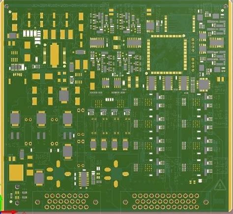
A brief discussion of common welding defects of circuit boards in common defects of PCB boards
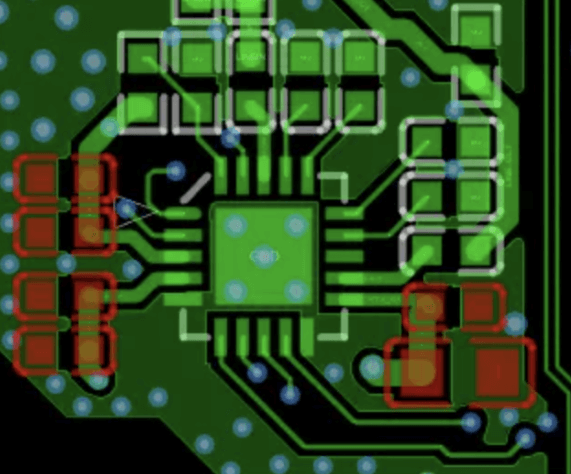
When we make PCBs, there are many common welding defects of circuit boards. The following figure shows the common sixteen welding defects.
The following is a detailed description of common welding defects, appearance characteristics, hazards, and cause analysis.
1.Cold soldering
(1)Appearance characteristics
There is an obvious black boundary between the solder and the component leads or the copper foil, and the solder is concave toward the boundary.
(2)Hazards
Cannot work normally.
(3)Cause analysis
1) The component leads are not cleaned well, not tinned or oxidized.
2) The printed circuit board is not cleaned well, and the quality of the sprayed flux is not good.
2.Solder accumulation
(1)Appearance characteristics
The solder joint structure is loose, white, and dull.
(2)Hazards
Insufficient mechanical strength may cause cold soldering.
(3)Cause analysis
1) The solder quality is poor.
2) The welding temperature is not enough.
3) The component leads are loose when the solder is not solidified.

3.Too much solder
(1)Appearance characteristics
The solder surface is convex.
(2)Hazards
Waste of solder and may contain defects.
(3)Cause analysis
Solder is withdrawn too late.
4.Too little solder
(1)Appearance characteristics
The soldering area is less than 80% of the pad, and the solder does not form a smooth transition surface.
(2)Hazards
Insufficient mechanical strength.
(3)Cause analysis
1) Poor solder fluidity or premature solder withdrawal.
2) Insufficient flux.
3) Too short welding time.
5.Rosin welding
(1)Appearance characteristics
Rosin slag is sandwiched in the weld.
(2)Hazards
Insufficient strength, poor conduction, and may be intermittent.
(3)Cause analysis
1) Too many welders or they have failed.
2) Insufficient welding time and insufficient heating.
3) The surface oxide film has not been removed.
6. Overheating
(1)Appearance characteristics
The solder joint is whitish, has no metallic luster, and has a rough surface.
(2)Hazards
The solder pad is easy to peel off and the strength is reduced.
(3)Cause analysis
The soldering iron power is too large and the heating time is too long.
7. Cold welding
(1)Appearance characteristics
The surface is in the shape of tofu dregs, and sometimes there may be cracks.
(2)Hazards
Low strength and poor conductivity.
(3)Cause analysis
The solder shakes before solidification.
7.Poor wetting
(1)Appearance characteristics
The interface between the solder and the weldment is too large and not smooth.
(2)Hazards
Low strength, no connection or intermittent connection.
(3)Cause analysis
1) The weldment is not cleaned properly.
2) Insufficient or poor quality flux.
3) The weldment is not fully heated.

9. Asymmetry
(1)Appearance characteristics
The solder does not flow all over the pad.
(2)Hazards
Insufficient strength.
(3)Cause analysis
1) Poor solder fluidity.
2) Insufficient or poor quality flux.
3) Insufficient heating.
10. Looseness
(1)Appearance characteristics
The wire or component lead can move.
(2)Hazards
Poor or no conduction.
(3)Cause analysis
1) The lead moves before the solder solidifies, causing gaps.
2) The lead is not processed well (poor wetting or no wetting).
11 Pull tip
(1)Appearance characteristics
The tip appears.
(2)Hazards
Poor appearance, easy to cause bridging.
(3)Cause analysis
1) Too little flux and too long heating time.
2) Improper soldering iron withdrawal angle.
12. Bridging
(1)Appearance characteristics
Adjacent wires are connected.
(2)Hazards
Electrical short circuit.
(3)Cause Analysis
1) Too much solder.
2) Improper soldering iron withdrawal angle.
Common defects, hazards, and cause analysis of circuit board welding
13.Pinholes
(1)Appearance characteristics
Holes can be seen by visual inspection or low-power magnifier.
(2)Hazards
Insufficient strength, solder joints are prone to corrosion.
(3)|Cause Analysis
The gap between the lead and the pad hole is too large.
14.Bubbles
(1)Appearance characteristics
There is a flame-like solder bulge at the root of the lead, and there is a cavity inside.
(2)Hazards
Temporary conduction, but it is easy to cause poor conduction for a long time.
(3)Cause Analysis
1) The gap between the lead and the pad hole is large.
2) Poor lead wetting.
3) The double-sided board plugging through-hole welding time is long, and the air in the hole expands.
15.Copper foil warping
(1)Appearance characteristics
The copper foil is peeled off from the printed board.
(2)Hazards
The printed board is damaged.
(3)Cause Analysis
The welding time is too long and the temperature is too high.
16.Peeling
(1)Appearance characteristics
The solder joint peels off from the copper foil (not the copper foil and the printed circuit board).
(2)Hazards
Open circuit.
(3)Cause Analysis
Poor metal plating on the pad.