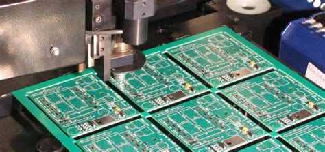
A brief discussion on the causes of blistering on the copper-plated circuit board
Blistering is one of the more common quality defects in the production process of circuit boards. The complexity of the production process and process maintenance of circuit boards, especially in chemical wet treatment, makes it difficult to prevent blistering defects on the board surface. Based on many years of actual production experience and service experience, the author now briefly analyzes the causes of blistering on the copper-plated circuit board surface, hoping to help colleagues in the industry!
Blistering on the circuit board surface is actually the problem of poor bonding strength of the board surface, and then extended to the surface quality of the board surface, which includes two aspects:
1.The problem of board surface cleanliness;
2.The problem of surface micro-roughness (or surface energy);
All blistering problems on the circuit board can be summarized as the above reasons. The bonding strength between the coatings is poor or too low, and it is difficult to resist the coating stress, mechanical stress and thermal stress generated during the production and processing process and assembly process, which ultimately causes different degrees of separation between the coatings.
Now, some factors that may cause poor board quality during the production and processing are summarized as follows:
3.Problems with substrate processing; especially for some thinner substrates (generally less than 0.8mm),
because the substrate has poor rigidity, it is not suitable to use a brushing machine to brush the board, which may not effectively remove the protective layer specially treated during the production and processing of the substrate to prevent the copper foil on the board from oxidizing. Although this layer is thin and easy to remove by brushing, it is more difficult to use chemical treatment. Therefore, it is important to pay attention to control during production and processing to avoid blistering caused by poor bonding between the copper foil of the board substrate and the chemical copper; this problem will also cause poor blackening and browning, uneven color, and local blackening and browning when the thin inner layer is blackened.
4.The board surface is poorly treated due to oil or other liquid contamination and dust pollution during machining (drilling, lamination, milling, etc.),
5.Poor copper brushing:
The pressure of the grinding plate before copper deposition is too large, causing the hole mouth to deform, brushing out the fillet of the hole mouth copper foil or even leaking the base material at the hole mouth, which will cause blistering at the hole mouth during copper deposition, electroplating, tin spraying, welding, etc.; Even if the brushing plate does not cause leakage of the base material, the overly heavy brushing plate will increase the roughness of the hole mouth copper, so the copper foil at this place is very likely to be over-roughened during the micro-etching and coarsening process, and there will be certain quality risks; Therefore, it is necessary to strengthen the control of the brushing plate process, and the brushing plate process parameters can be adjusted to the best through the wear mark test and water film test;
6.Water washing problem:
Because copper plating treatment requires a lot of chemical treatment, there are many kinds of acid, alkali, non-polar organic and other chemical solvents. If the board surface is not washed clean, especially the copper plating adjustment degreasing agent, it will not only cause cross contamination, but also cause local poor treatment or poor treatment effect of the board surface, uneven defects, and some problems in bonding strength; therefore, attention should be paid to strengthening the control of water washing, mainly including the control of the flow rate, water quality, washing time, and dripping time of the cleaning water; especially in winter when the temperature is low, the washing effect will be greatly reduced, and more attention should be paid to strengthening the control of water washing;
7.Micro-etching in copper pre-treatment and graphic electroplating pre-treatment;
excessive micro-etching will cause the hole mouth to leak the substrate and cause blistering around the hole mouth; insufficient micro-etching will also cause insufficient bonding and cause blistering; therefore, it is necessary to strengthen the control of micro-etching; generally, the micro-etching depth of copper pre-treatment is 1.5-2 microns, and the micro-etching depth of graphic electroplating pre-treatment is 0.3-1 microns. If conditions permit, it is best to control the micro-etching thickness or etching rate through chemical analysis and simple experimental weighing method; generally, the color of the board after micro-etching is bright, uniform pink, and there is no reflection; if the color is uneven, or there is reflection, it means that there are quality risks in the pre-processing; pay attention to strengthen inspection; in addition, the copper content of the micro-etching tank, the tank liquid temperature, the load, the micro-etching agent content, etc. are all items to pay attention to;
8.The activity of the copper plating solution is too strong;
the content of the three major components in the newly opened copper plating solution or the bath is too high,
especially the copper content is too high, which will cause the bath liquid to be too active, the chemical copper deposition is rough, and the excessive inclusion of hydrogen, cuprous oxide, etc. in the chemical copper layer will cause the physical properties of the coating to deteriorate and the bonding strength is poor; the following methods can be appropriately adopted: reduce the copper content (add pure water to the bath liquid), including the three major components, appropriately increase the content of complexing agent and stabilizer, appropriately reduce the temperature of the bath liquid, etc.;
9.The board surface is oxidized during the production process;
if the copper plating board is oxidized in the air, it may not only cause no copper in the hole, the board surface is rough, but also cause blistering on the board surface; if the copper plating board is stored in the acid solution for too long, the board surface will also oxidize, and this oxide film is difficult to remove; therefore, during the production process, the copper plating board should be thickened in time, and it should not be stored for too long. Generally, the thickening and copper plating should be completed within 12 hours at the latest;
10.Poor copper plating rework;
some reworked boards after copper plating or pattern transfer will cause blistering on the board surface during the rework process due to poor deplating, incorrect rework method or improper micro-etching time control during the rework process or other reasons; if the copper plating of the copper plating board is found to be poor on the line, it can be directly degreased from the line after water washing and then pickled without etching and reworked directly; it is best not to degrease and micro-etch again; for the boards that have been thickened by the board, they should be deplated in the micro-etching tank now, and pay attention to time control. You can use one or two boards to roughly calculate the deplating time to ensure the deplating effect; after deplating, use a set of soft grinding brushes behind the brush machine to brush lightly and then deposit copper according to the normal production process, but the micro-etching time should be halved or adjusted as necessary;
11.Insufficient water washing after development during pattern transfer,
too long storage time after development or too much dust in the workshop will cause poor board surface cleanliness and slightly poor fiber treatment effect, which may cause potential quality problems;
12.Before copper plating, the acid bath should be replaced in time.
Too much pollution in the bath liquid or too high copper content will not only cause problems with the cleanliness of the board surface, but also cause defects such as rough board surface;
13.Organic pollution, especially oil pollution, appears in the electroplating tank, which is more likely to occur for automatic lines;
14.In addition, in winter, when the bath liquid is not heated in some factories during production,
special attention should be paid to the charged entry of the board into the tank during the production process, especially for plating tanks with air stirring, such as copper-nickel; for nickel cylinders, it is best to add a heated water washing tank before nickel plating in winter (the water temperature is about 30-40 degrees) to ensure that the initial deposition of the nickel layer is dense and good;
In the actual production process, there are many reasons for the blistering of the board surface. The author can only make a brief analysis. Different manufacturers’ equipment and technical levels may cause blistering phenomena due to different reasons. The specific situation should be analyzed specifically, and it cannot be generalized or applied mechanically. The above reasons are analyzed regardless of priority and importance. A brief analysis is basically made according to the production process. In this series, it is just to provide everyone with a direction to solve the problem and a broader vision. I hope it can play a role in inspiring others in your process production and problem solving!